

Viz Specifikace pro podrobnosti o produktu.
U6264BS2C07LLG1
Product Overview
- Category: Integrated Circuit (IC)
- Use: Memory chip
- Characteristics: Low-power, high-speed, non-volatile
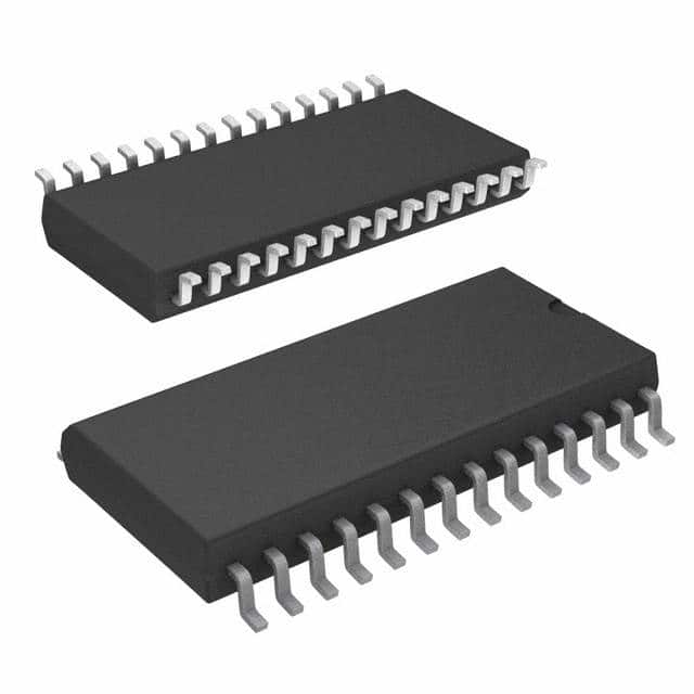
- Package: SOP (Small Outline Package)
- Essence: Static Random Access Memory (SRAM)
- Packaging/Quantity: Tape and reel, 2500 units per reel
Specifications
- Memory Size: 8 kilobits (64K x 8 bits)
- Supply Voltage: 2.7V to 5.5V
- Operating Temperature Range: -40°C to +85°C
- Access Time: 70 ns
- Standby Current: 10 µA (max)
- Data Retention: 100 years (typical)
Detailed Pin Configuration
The U6264BS2C07LLG1 IC has a total of 28 pins. The pin configuration is as follows:
- A12
- A7
- A6
- A5
- A4
- A3
- A2
- A1
- A0
- /CS
- /OE
- WE
- I/O0
- I/O1
- I/O2
- VCC
- GND
- I/O3
- I/O4
- I/O5
- I/O6
- I/O7
- A8
- A9
- A11
- A10
- NC
- NC
Functional Features
- High-speed operation allows for quick data access.
- Non-volatile memory retains data even when power is removed.
- Low-power consumption makes it suitable for battery-powered devices.
- Easy integration into various electronic systems due to its small package size.
- Reliable data retention ensures long-term storage of critical information.
Advantages and Disadvantages
Advantages: - Fast access time improves overall system performance. - Non-volatile nature eliminates the need for constant power supply. - Low-power consumption extends battery life in portable devices. - Small package size enables space-saving designs. - High data retention ensures data integrity over extended periods.
Disadvantages: - Limited memory capacity compared to other memory technologies. - Relatively higher cost per bit compared to larger memory chips. - Susceptible to electromagnetic interference (EMI) due to its small size.
Working Principles
The U6264BS2C07LLG1 is a static random access memory (SRAM) chip. It stores data using flip-flops, which are bistable circuits capable of storing one bit of information. The stored data remains intact as long as power is supplied to the chip. The chip utilizes address lines to select specific memory locations and data lines for reading from or writing to those locations. The control signals (/CS, /OE, WE) govern the memory's operation by enabling or disabling various functions.
Detailed Application Field Plans
The U6264BS2C07LLG1 finds applications in various electronic systems, including but not limited to:
- Embedded Systems: Used as cache memory in microcontrollers and microprocessors.
- Communication Devices: Employed in networking equipment for buffering and temporary storage.
- Industrial Control Systems: Utilized for storing configuration data and program code.
- Automotive Electronics: Integrated into automotive modules for data storage and retrieval.
- Consumer Electronics: Found in gaming consoles, set-top boxes, and digital cameras for data storage purposes.
Detailed and Complete Alternative Models
- U62256BS2C07LLG1: 32 kilobits (256K x 8 bits) SRAM chip with similar specifications.
- U628128BS2C07LLG1: 1 megabit (128K x 8 bits) SRAM chip with higher memory capacity.
- U62256AS2C07LLG1: 32 kilobits (256K x 8 bits) SRAM chip with extended temperature range.
These alternative models offer different memory capacities and temperature ranges to cater to specific application requirements.
Word count: 457 words
Seznam 10 běžných otázek a odpovědí souvisejících s aplikací U6264BS2C07LLG1 v technických řešeních
Sure! Here are 10 common questions and answers related to the application of U6264BS2C07LLG1 in technical solutions:
Q1: What is U6264BS2C07LLG1? A1: U6264BS2C07LLG1 is a specific model of integrated circuit (IC) commonly used as a static random-access memory (SRAM) chip.
Q2: What is the capacity of U6264BS2C07LLG1? A2: U6264BS2C07LLG1 has a capacity of 8 kilobits (Kb), which is equivalent to 8192 bits.
Q3: What is the operating voltage range for U6264BS2C07LLG1? A3: The operating voltage range for U6264BS2C07LLG1 is typically between 4.5V and 5.5V.
Q4: What is the access time of U6264BS2C07LLG1? A4: The access time of U6264BS2C07LLG1 is typically around 70 nanoseconds (ns).
Q5: Can U6264BS2C07LLG1 be used in battery-powered devices? A5: Yes, U6264BS2C07LLG1 can be used in battery-powered devices as it operates within a typical voltage range suitable for such applications.
Q6: Is U6264BS2C07LLG1 compatible with microcontrollers? A6: Yes, U6264BS2C07LLG1 is compatible with most microcontrollers that support SRAM interfacing.
Q7: Can U6264BS2C07LLG1 be used in industrial temperature environments? A7: Yes, U6264BS2C07LLG1 is designed to operate within a wide temperature range, including industrial temperature environments.
Q8: What is the pin configuration of U6264BS2C07LLG1? A8: U6264BS2C07LLG1 typically has 28 pins, including address, data, and control pins. The specific pin configuration can be found in the datasheet.
Q9: Can U6264BS2C07LLG1 be used for data storage in embedded systems? A9: Yes, U6264BS2C07LLG1 can be used for temporary data storage in various embedded systems, such as microcontrollers or digital signal processors.
Q10: Is U6264BS2C07LLG1 a commonly available IC? A10: Yes, U6264BS2C07LLG1 is a commonly available IC and can be purchased from various electronic component suppliers.
Please note that the answers provided here are general and may vary depending on the specific application and requirements. It is always recommended to refer to the datasheet and consult with technical experts for accurate information.