

Viz Specifikace pro podrobnosti o produktu.
AD7225LN
Product Overview
- Category: Integrated Circuit (IC)
- Use: Digital-to-Analog Converter (DAC)
- Characteristics: High-resolution, low-power consumption
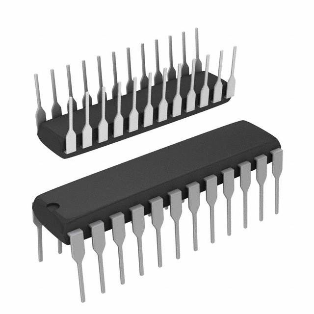
- Package: DIP (Dual In-line Package)
- Essence: Converts digital signals into analog voltages
- Packaging/Quantity: Tube packaging, 25 pieces per tube
Specifications
- Resolution: 8 bits
- Number of Channels: 1
- Supply Voltage: +5V
- Power Consumption: 10mW
- Output Voltage Range: 0V to Vref
- Reference Voltage: External or internal
- Operating Temperature Range: -40°C to +85°C
Detailed Pin Configuration
The AD7225LN has a total of 20 pins. The pin configuration is as follows:
- VOUT
- AGND
- DGND
- VREF
- VDD
- DB7
- DB6
- DB5
- DB4
- DB3
- DB2
- DB1
- DB0
- WR
- CS
- CLK
- A0
- A1
- A2
- RESET
Functional Features
- High-resolution DAC with 8-bit resolution
- Low power consumption for energy-efficient operation
- Wide output voltage range allows for versatile applications
- Can be used with external or internal reference voltage
- Easy interfacing with microcontrollers and other digital systems
Advantages and Disadvantages
Advantages: - High resolution provides accurate analog outputs - Low power consumption extends battery life in portable devices - Versatile output voltage range suits various applications - Compatible with different reference voltage sources - Simple integration with digital systems
Disadvantages: - Limited to single-channel output - Requires external components for complete functionality - May require additional circuitry for noise reduction
Working Principles
The AD7225LN is a digital-to-analog converter that converts digital signals into corresponding analog voltages. It utilizes an 8-bit resolution to provide precise analog outputs. The input digital data is received through the DB0-DB7 pins, and the WR (Write) pin is used to latch the data. The CS (Chip Select) pin enables or disables the device. The CLK (Clock) pin synchronizes the conversion process.
The reference voltage, VREF, determines the maximum output voltage range. It can be provided externally or generated internally. The DAC generates an analog output voltage proportional to the digital input code. This analog voltage is available at the VOUT pin.
Detailed Application Field Plans
The AD7225LN finds applications in various fields, including:
- Industrial Automation: Control systems requiring accurate analog outputs.
- Audio Equipment: Digital audio processing and sound synthesis.
- Instrumentation: Measurement and testing equipment.
- Communication Systems: Analog signal generation for modulation.
- Robotics: Precise control of robotic movements.
- Automotive Electronics: Vehicle control systems and infotainment.
Detailed and Complete Alternative Models
- AD7303: 8-bit DAC with dual-channel output.
- AD5628: 12-bit DAC with single-channel output.
- AD5669: 16-bit DAC with quad-channel output.
- AD5754: 18-bit DAC with single-channel output.
- AD5767: 20-bit DAC with dual-channel output.
These alternative models offer different resolutions, channel configurations, and features to suit specific application requirements.
Word count: 410 words
Seznam 10 běžných otázek a odpovědí souvisejících s aplikací AD7225LN v technických řešeních
Sure! Here are 10 common questions and answers related to the application of AD7225LN in technical solutions:
Q: What is AD7225LN? A: AD7225LN is a digital-to-analog converter (DAC) chip that converts digital signals into analog voltages.
Q: What is the resolution of AD7225LN? A: AD7225LN has a resolution of 8 bits, meaning it can represent 256 different voltage levels.
Q: What is the supply voltage range for AD7225LN? A: The supply voltage range for AD7225LN is typically between +5V and +15V.
Q: Can AD7225LN be used with microcontrollers? A: Yes, AD7225LN can be easily interfaced with microcontrollers using standard digital communication protocols like SPI or I2C.
Q: How many channels does AD7225LN have? A: AD7225LN has 4 independent analog output channels, allowing you to control up to 4 different analog devices.
Q: What is the settling time of AD7225LN? A: The settling time of AD7225LN is typically around 10 microseconds, ensuring fast and accurate voltage outputs.
Q: Can AD7225LN handle negative voltages? A: No, AD7225LN is designed to work with positive voltages only. It cannot generate or handle negative voltages.
Q: What is the maximum output current of AD7225LN? A: AD7225LN can provide a maximum output current of 5 mA per channel.
Q: Is AD7225LN suitable for precision applications? A: While AD7225LN offers good accuracy and performance, it may not be suitable for high-precision applications due to its 8-bit resolution.
Q: Can AD7225LN be used in industrial environments? A: Yes, AD7225LN is designed to operate reliably in industrial environments with a wide temperature range and robustness against noise and interference.
Please note that these answers are general and may vary depending on the specific application and requirements.