

Viz Specifikace pro podrobnosti o produktu.
AD7549JP
Product Overview
Category
AD7549JP belongs to the category of digital-to-analog converters (DACs).
Use
It is used to convert digital signals into analog signals.
Characteristics
- High precision and accuracy
- Fast conversion speed
- Low power consumption
- Wide operating temperature range
Package
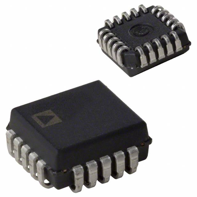
AD7549JP comes in a 20-pin plastic dual in-line package (DIP).
Essence
The essence of AD7549JP lies in its ability to accurately convert digital data into corresponding analog voltages.
Packaging/Quantity
AD7549JP is typically packaged in reels or tubes, with a quantity of 25 units per package.
Specifications
- Resolution: 12 bits
- Supply Voltage: +5V
- Operating Temperature Range: -40°C to +85°C
- Conversion Time: 10µs
- Output Voltage Range: 0V to Vref
Detailed Pin Configuration
- VDD - Power supply voltage
- VREF - Reference voltage input
- AGND - Analog ground
- DGND - Digital ground
- WR - Write control input
- RD - Read control input
- CS - Chip select input
- A0-A11 - Address inputs
- D0-D7 - Data inputs
- OUT - Analog output
- REFOUT - Reference output 12-20. NC - No connection
Functional Features
- High linearity and accuracy in converting digital data to analog voltages
- On-chip reference voltage generator for improved performance
- Serial interface for easy integration with microcontrollers
- Low glitch energy for minimal signal distortion
- Power-down mode for reduced power consumption during idle periods
Advantages
- Precise and reliable conversion of digital signals to analog voltages
- Fast conversion speed enables real-time applications
- Low power consumption for energy-efficient operation
- Wide operating temperature range allows usage in various environments
Disadvantages
- Limited resolution of 12 bits may not be sufficient for certain high-precision applications
- Requires an external reference voltage source for accurate conversions
Working Principles
AD7549JP utilizes a combination of digital circuitry and analog components to convert digital data into corresponding analog voltages. The digital input signals are processed internally, and the resulting analog output voltage is proportional to the digital input value.
Detailed Application Field Plans
AD7549JP finds application in various fields, including:
- Industrial automation: Control systems requiring precise analog outputs.
- Audio equipment: Digital audio-to-analog conversion for high-fidelity sound reproduction.
- Instrumentation: Measurement devices requiring accurate analog outputs.
- Communication systems: Analog signal generation for modulation and demodulation processes.
- Automotive electronics: Control modules requiring analog voltage outputs.
Detailed and Complete Alternative Models
- AD7541 - 10-bit DAC with similar features but lower resolution.
- AD7545 - 12-bit DAC with improved performance and additional features.
- AD7543 - 8-bit DAC with reduced resolution but lower cost.
These alternative models offer different trade-offs in terms of resolution, performance, and cost, allowing users to choose the most suitable option for their specific requirements.
Word count: 513 words
Seznam 10 běžných otázek a odpovědí souvisejících s aplikací AD7549JP v technických řešeních
Sure! Here are 10 common questions and answers related to the application of AD7549JP in technical solutions:
Q: What is AD7549JP? A: AD7549JP is a digital-to-analog converter (DAC) chip manufactured by Analog Devices.
Q: What is the resolution of AD7549JP? A: AD7549JP has a resolution of 12 bits, meaning it can convert digital input into analog output with 4096 possible levels.
Q: What is the operating voltage range for AD7549JP? A: AD7549JP operates within a voltage range of +5V to +15V.
Q: Can AD7549JP handle both unipolar and bipolar outputs? A: No, AD7549JP only supports unipolar output voltages ranging from 0V to Vref.
Q: What is the maximum settling time for AD7549JP? A: The maximum settling time for AD7549JP is typically 10 microseconds.
Q: Does AD7549JP have an internal reference voltage? A: No, AD7549JP requires an external reference voltage (Vref) for proper operation.
Q: What is the power supply current requirement for AD7549JP? A: AD7549JP typically consumes around 2mA of power supply current.
Q: Can AD7549JP operate in harsh environments? A: AD7549JP is not specifically designed for harsh environments and may require additional protection measures.
Q: Is AD7549JP suitable for high-speed applications? A: AD7549JP is not optimized for high-speed applications and may have limitations in terms of bandwidth.
Q: What are some typical applications of AD7549JP? A: AD7549JP is commonly used in various industrial control systems, process automation, motor control, and instrumentation applications.
Please note that the answers provided here are general and may vary depending on specific requirements and use cases.