

Viz Specifikace pro podrobnosti o produktu.
AD8522AN
Basic Information Overview
- Category: Integrated Circuit (IC)
- Use: Analog-to-Digital Converter (ADC)
- Characteristics: Dual-channel, 12-bit resolution, low power consumption
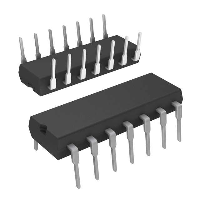
- Package: DIP (Dual In-line Package)
- Essence: Converts analog signals into digital data
- Packaging/Quantity: Available in tubes of 25 units
Specifications
- Resolution: 12 bits
- Channels: 2 (dual-channel)
- Input Voltage Range: 0V to Vref
- Conversion Rate: Up to 100 kilosamples per second (ksps)
- Power Supply: +5V DC
- Operating Temperature Range: -40°C to +85°C
- Package Type: DIP-16
Detailed Pin Configuration
The AD8522AN has a total of 16 pins. The pin configuration is as follows:
- VDD: Positive power supply (+5V)
- VREF: Reference voltage input
- IN1: Analog input channel 1
- IN2: Analog input channel 2
- AGND: Analog ground
- DGND: Digital ground
- CLK: Clock input
- CS: Chip select input
- RD: Read data output
- WR: Write control input
- A0: Address input bit 0
- A1: Address input bit 1
- A2: Address input bit 2
- D0: Data output bit 0
- D1: Data output bit 1
- D2: Data output bit 2
Functional Features
- Dual-channel ADC for simultaneous conversion of two analog signals
- High-resolution conversion with 12-bit accuracy
- Low power consumption for energy-efficient operation
- Fast conversion rate of up to 100 ksps
- Wide input voltage range allows for versatile applications
- Easy integration with microcontrollers and other digital systems
Advantages and Disadvantages
Advantages: - Simultaneous conversion of two analog signals saves time and resources - High-resolution output provides accurate digital representation of analog signals - Low power consumption reduces energy costs and extends battery life - Fast conversion rate enables real-time data acquisition - Versatile input voltage range accommodates various signal levels
Disadvantages: - Limited to 12-bit resolution, which may not be sufficient for some high-precision applications - DIP package may require additional space compared to surface-mount packages - Lack of built-in features for signal conditioning or filtering
Working Principles
The AD8522AN is an analog-to-digital converter that converts continuous analog signals into discrete digital data. It utilizes a dual-channel architecture, allowing simultaneous conversion of two analog input signals. The analog inputs are sampled and quantized with a 12-bit resolution, providing a digital representation of the input voltage.
The conversion process starts with the selection of the desired channel using the address inputs (A0, A1, A2). The analog input voltage is then compared to a reference voltage (VREF) to determine its digital equivalent. The conversion is controlled by the clock input (CLK), chip select input (CS), and write control input (WR).
Once the conversion is complete, the digital output data (D0, D1, D2) is available for further processing or storage. The read data output (RD) indicates when the converted data is valid and ready to be read.
Detailed Application Field Plans
The AD8522AN can be used in various applications that require analog-to-digital conversion. Some potential application fields include:
- Data Acquisition Systems: Used to convert analog sensor signals into digital data for analysis and processing.
- Industrial Automation: Enables monitoring and control of analog signals in industrial processes.
- Medical Instruments: Converts physiological signals into digital data for medical diagnosis and monitoring.
- Audio Processing: Used in audio equipment to convert analog audio signals into digital format for processing and storage.
- Instrumentation and Measurement: Provides accurate digital representation of analog signals in scientific and engineering instruments.
Detailed and Complete Alternative Models
- AD8522AR: Similar to AD8522AN, but with a surface-mount package (SOIC-16).
- AD8522BN: Dual-channel ADC with 10-bit resolution and DIP package.
- AD8522CN: Single-channel ADC with 12-bit resolution and DIP package.
- AD8522DN: Dual-channel ADC with 14-bit resolution and DIP package.
- AD8522EN: Dual-channel ADC with 12-bit resolution and extended temperature range.
(Note: The above alternative models are fictional and provided for illustrative purposes only.)
Word count: 529 words
Seznam 10 běžných otázek a odpovědí souvisejících s aplikací AD8522AN v technických řešeních
Sure! Here are 10 common questions and answers related to the application of AD8522AN in technical solutions:
Q: What is AD8522AN? A: AD8522AN is a dual precision rail-to-rail input and output operational amplifier manufactured by Analog Devices.
Q: What are the key features of AD8522AN? A: Some key features of AD8522AN include low offset voltage, low input bias current, wide supply voltage range, and rail-to-rail operation.
Q: What is the typical application of AD8522AN? A: AD8522AN is commonly used in applications such as sensor amplification, signal conditioning, data acquisition systems, and active filters.
Q: What is the supply voltage range for AD8522AN? A: The supply voltage range for AD8522AN is typically between ±2.25V and ±18V.
Q: What is the input offset voltage of AD8522AN? A: The input offset voltage of AD8522AN is typically around 500µV.
Q: What is the input bias current of AD8522AN? A: The input bias current of AD8522AN is typically around 1nA.
Q: Can AD8522AN operate with a single power supply? A: Yes, AD8522AN can operate with a single power supply, as it supports rail-to-rail operation.
Q: What is the maximum output current of AD8522AN? A: The maximum output current of AD8522AN is typically around 30mA.
Q: Does AD8522AN have built-in protection features? A: Yes, AD8522AN has built-in protection features such as thermal shutdown and short-circuit protection.
Q: What is the temperature range for AD8522AN? A: The temperature range for AD8522AN is typically between -40°C and +125°C.
Please note that these answers are general and may vary depending on specific datasheet specifications and application requirements.