

Viz Specifikace pro podrobnosti o produktu.
AD9739ABBCZRL
Product Overview
- Category: Integrated Circuit (IC)
- Use: Digital-to-Analog Converter (DAC)
- Characteristics:
- High-speed and high-resolution DAC
- Low power consumption
- Small form factor
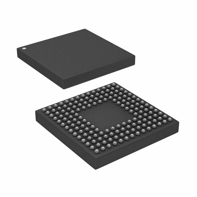
- Package: BGA (Ball Grid Array)
- Essence: Converts digital signals into analog signals
- Packaging/Quantity: Available in reels of 250 units
Specifications
- Resolution: 14 bits
- Sampling Rate: Up to 1 GSPS (Giga Samples Per Second)
- Power Supply: 3.3V
- Operating Temperature Range: -40°C to +85°C
- Output Voltage Range: 0V to 2.5V
- Differential Nonlinearity (DNL): ±0.5 LSB (Least Significant Bit)
- Integral Nonlinearity (INL): ±1 LSB
Pin Configuration
The AD9739ABBCZRL has a total of 64 pins, which are arranged as follows:
```
Pin Name Description
1 VDD Power Supply 2 VDD Power Supply 3 VREFP Positive Reference Voltage 4 VREFN Negative Reference Voltage 5 AGND Analog Ground 6 DVDD Digital Power Supply 7 DGND Digital Ground 8 CLK Clock Input 9 DATA Digital Data Input 10 RESET Reset Input 11 FSADJ Full-Scale Adjust 12 PDWN Power-Down Control 13 SYNC Synchronization Input 14 REFCLK Reference Clock Input 15 REFA Reference Voltage A 16 REFB Reference Voltage B ... ... ... 64 VDD Power Supply ```
Functional Features
- High-speed digital-to-analog conversion
- Low power consumption for energy-efficient operation
- Wide output voltage range for versatile applications
- Adjustable full-scale range for precise control
- Synchronization input for accurate timing
Advantages and Disadvantages
Advantages: - High resolution and sampling rate - Small form factor for space-constrained designs - Low power consumption for energy efficiency
Disadvantages: - Limited output voltage range compared to some other DACs - Requires external reference voltages for operation
Working Principles
The AD9739ABBCZRL is a digital-to-analog converter that converts digital signals into analog signals. It operates by taking in digital data and using an internal clock to sample and convert the data into analog voltage levels. The converted analog signal can then be used for various applications such as audio processing, waveform generation, or communication systems.
Detailed Application Field Plans
The AD9739ABBCZRL is commonly used in the following application fields:
- Communications: Used in wireless base stations, software-defined radios, and high-speed data transmission systems.
- Test and Measurement: Utilized in signal generators, arbitrary waveform generators, and high-speed data acquisition systems.
- Audio Processing: Integrated into professional audio equipment, digital mixing consoles, and audio effects processors.
- Radar Systems: Employed in radar signal generation, target simulation, and radar testing equipment.
Detailed and Complete Alternative Models
- AD9738ABBCZRL: Similar to AD9739ABBCZRL but with a lower resolution of 12 bits.
- AD9737ABBCZRL: Lower resolution (10 bits) version of AD9739ABBCZRL.
- AD9736ABBCZRL: Lower resolution (8 bits) version of AD9739ABBCZRL.
These alternative models provide options with different resolutions to suit specific application requirements.
Word count: 470 words
Seznam 10 běžných otázek a odpovědí souvisejících s aplikací AD9739ABBCZRL v technických řešeních
Sure! Here are 10 common questions and answers related to the application of AD9739ABBCZRL in technical solutions:
Q: What is the AD9739ABBCZRL? A: The AD9739ABBCZRL is a high-speed digital-to-analog converter (DAC) designed for various applications, including wireless communications, instrumentation, and defense systems.
Q: What is the maximum sampling rate of the AD9739ABBCZRL? A: The AD9739ABBCZRL supports a maximum sampling rate of 2.5 GSPS (giga-samples per second).
Q: What is the resolution of the AD9739ABBCZRL? A: The AD9739ABBCZRL has a resolution of 14 bits, providing excellent signal fidelity.
Q: Can the AD9739ABBCZRL be used in multi-carrier applications? A: Yes, the AD9739ABBCZRL is suitable for multi-carrier applications due to its wide bandwidth and high dynamic range.
Q: Does the AD9739ABBCZRL require an external reference clock? A: Yes, the AD9739ABBCZRL requires an external reference clock for proper operation.
Q: What is the power supply voltage range for the AD9739ABBCZRL? A: The AD9739ABBCZRL operates with a power supply voltage range of 1.8V to 3.3V.
Q: Can the AD9739ABBCZRL interface directly with FPGA or microcontrollers? A: Yes, the AD9739ABBCZRL features a high-speed JESD204B interface, allowing direct interfacing with FPGAs or microcontrollers.
Q: What is the typical power consumption of the AD9739ABBCZRL? A: The AD9739ABBCZRL has a typical power consumption of 1.5W, making it suitable for power-sensitive applications.
Q: Does the AD9739ABBCZRL support digital gain and offset control? A: Yes, the AD9739ABBCZRL provides digital gain and offset control to optimize signal performance.
Q: Are evaluation boards available for the AD9739ABBCZRL? A: Yes, Analog Devices offers evaluation boards for the AD9739ABBCZRL, allowing users to easily test and evaluate its performance in their specific applications.
Please note that these answers are general and may vary depending on the specific requirements and implementation of the AD9739ABBCZRL in different technical solutions.