

Viz Specifikace pro podrobnosti o produktu.
DAC8143FS
Product Overview
Category: Digital-to-Analog Converter (DAC)
Use: The DAC8143FS is a high-performance digital-to-analog converter designed for various applications that require precise analog output signals. It is commonly used in audio equipment, industrial automation systems, telecommunications, and instrumentation.
Characteristics: - High resolution: The DAC8143FS provides a resolution of up to 14 bits, ensuring accurate conversion of digital data into analog signals. - Low power consumption: This DAC operates at low power levels, making it suitable for battery-powered devices and energy-efficient applications. - Fast settling time: With a fast settling time of less than 10 microseconds, the DAC8143FS can quickly respond to changes in input data, enabling real-time signal generation. - Wide voltage range: It supports a wide supply voltage range of 2.7V to 5.5V, allowing compatibility with various power sources. - Small package size: The DAC8143FS is available in a compact package, making it suitable for space-constrained designs.
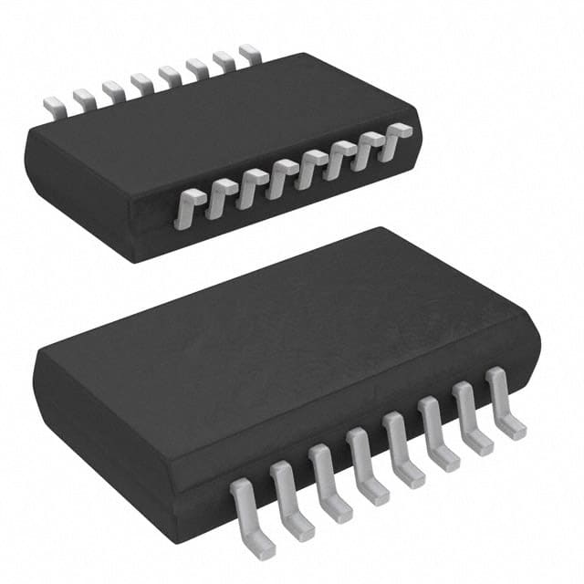
Package: The DAC8143FS is offered in a small form factor package, such as a QFN (Quad Flat No-Lead) or TSSOP (Thin Shrink Small Outline Package), ensuring ease of integration into different circuit boards.
Essence: The DAC8143FS is a key component in digital systems that require accurate analog outputs. It converts digital data into corresponding analog voltages, enabling precise control and manipulation of analog signals.
Packaging/Quantity: The DAC8143FS is typically sold in reels or trays, with quantities varying based on customer requirements. Common packaging options include tape and reel, containing several hundred units per reel.
Specifications
- Resolution: 14 bits
- Supply Voltage Range: 2.7V to 5.5V
- Settling Time: <10 microseconds
- Operating Temperature Range: -40°C to +85°C
- Output Voltage Range: 0V to Vref
Detailed Pin Configuration
The DAC8143FS features a standard pin configuration, as follows:
- VDD: Power supply voltage
- GND: Ground reference
- DIN: Serial data input
- SCLK: Serial clock input
- CS: Chip select input
- REF: Reference voltage input
- AGND: Analog ground
- OUT: Analog output
Functional Features
- High linearity: The DAC8143FS ensures high linearity in converting digital values to analog voltages, minimizing distortion and signal degradation.
- Low glitch energy: It exhibits low glitch energy during transitions, reducing unwanted noise and ensuring accurate signal reproduction.
- Power-on reset: The DAC8143FS includes a power-on reset circuit that initializes the device to a known state upon power-up, ensuring reliable operation.
- SPI interface: It utilizes a Serial Peripheral Interface (SPI) for easy integration with microcontrollers and other digital devices.
Advantages and Disadvantages
Advantages: - High resolution and accuracy - Low power consumption - Fast settling time - Wide voltage range - Compact package size - Easy integration with digital systems
Disadvantages: - Limited output voltage range (0V to Vref) - Requires external reference voltage source
Working Principles
The DAC8143FS operates by accepting digital input data and converting it into corresponding analog voltages. It utilizes an internal digital-to-analog conversion technique, which involves precise voltage generation based on the provided digital code. The converted analog signal is then available at the output pin for further processing or direct utilization.
Detailed Application Field Plans
The DAC8143FS finds applications in various fields, including:
- Audio Equipment: It is used in audio systems to generate accurate analog signals for amplification, filtering, and equalization purposes.
- Industrial Automation: The DAC8143FS enables precise control of analog actuators, such as motors and valves, in industrial automation systems.
- Telecommunications: It is utilized in telecommunications equipment for signal modulation, demodulation, and transmission purposes.
- Instrumentation: The DAC8143FS plays a crucial role in test and measurement instruments, providing accurate analog outputs for signal generation and calibration.
Detailed and Complete Alternative Models
- DAC8141FS: Similar to the DAC8143FS, but with a lower resolution of 12 bits.
- DAC8144FS: Offers higher resolution with 16 bits, suitable for applications requiring finer analog output precision.
- DAC8142FS: A dual-channel version of the DAC8143FS, providing two independent analog outputs.
These alternative models offer different resolutions and channel configurations, allowing users to choose the most suitable option based on their specific requirements.
Word count: 610 words
Seznam 10 běžných otázek a odpovědí souvisejících s aplikací DAC8143FS v technických řešeních
Sure! Here are 10 common questions and answers related to the application of DAC8143FS in technical solutions:
Q: What is DAC8143FS? A: DAC8143FS is a digital-to-analog converter (DAC) integrated circuit that converts digital signals into analog voltage or current outputs.
Q: What is the operating voltage range of DAC8143FS? A: The operating voltage range of DAC8143FS is typically between 2.7V and 5.5V.
Q: How many channels does DAC8143FS have? A: DAC8143FS has four independent channels, allowing for simultaneous conversion of multiple digital inputs to analog outputs.
Q: What is the resolution of DAC8143FS? A: DAC8143FS has a resolution of 14 bits, meaning it can provide 2^14 (16,384) different output levels.
Q: Can DAC8143FS be used for both voltage and current output applications? A: Yes, DAC8143FS can be configured to provide either voltage or current outputs, making it versatile for various applications.
Q: What is the maximum output current of DAC8143FS? A: The maximum output current of DAC8143FS is typically around 20 mA per channel.
Q: Does DAC8143FS support serial communication interfaces? A: Yes, DAC8143FS supports standard serial communication interfaces such as SPI (Serial Peripheral Interface) and I2C (Inter-Integrated Circuit).
Q: Can DAC8143FS operate in both single-ended and differential modes? A: Yes, DAC8143FS can operate in both single-ended and differential modes, providing flexibility in signal conditioning applications.
Q: Is DAC8143FS suitable for precision applications? A: Yes, DAC8143FS is designed with low integral non-linearity (INL) and differential non-linearity (DNL), making it suitable for precision applications.
Q: What are some typical applications of DAC8143FS? A: DAC8143FS can be used in various applications such as industrial automation, process control, motor control, audio equipment, and instrumentation.
Please note that the answers provided here are general and may vary depending on specific datasheet specifications and application requirements.