

Viz Specifikace pro podrobnosti o produktu.
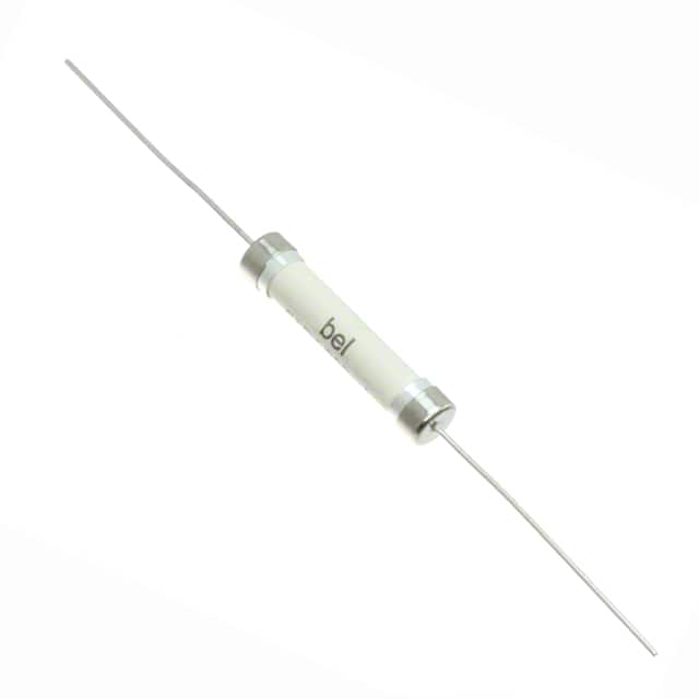
0ADBP0250-RE Product Overview
Introduction
The 0ADBP0250-RE is a versatile electronic component that belongs to the category of integrated circuits. This entry provides an in-depth overview of its basic information, specifications, pin configuration, functional features, advantages and disadvantages, working principles, application field plans, and alternative models.
Basic Information Overview
- Category: Integrated Circuit
- Use: The 0ADBP0250-RE is commonly used in electronic devices for signal processing, amplification, and control applications.
- Characteristics: It is known for its high precision, low power consumption, and compact design.
- Package: The 0ADBP0250-RE is typically available in a small outline integrated circuit (SOIC) package.
- Essence: This component plays a crucial role in enhancing the performance and functionality of electronic systems.
- Packaging/Quantity: It is usually supplied in reels or tubes containing multiple units.
Specifications
The detailed specifications of the 0ADBP0250-RE are as follows: - Input Voltage Range: 3V to 5.5V - Operating Temperature: -40°C to 85°C - Output Current: 100mA - Gain Bandwidth Product: 25MHz - Package Type: SOIC-8
Detailed Pin Configuration
The 0ADBP0250-RE features the following pin configuration: 1. VCC 2. GND 3. IN- 4. IN+ 5. OUT 6. NC 7. NC 8. NC
Functional Features
- High precision amplification
- Low input offset voltage
- Rail-to-rail output swing
- Low quiescent current
Advantages and Disadvantages
Advantages
- Wide input voltage range
- Enhanced precision and accuracy
- Versatile application potential
- Compact form factor
Disadvantages
- Limited output current capacity
- Sensitive to electromagnetic interference
Working Principles
The 0ADBP0250-RE operates based on the principles of operational amplifiers, utilizing differential input signals to provide precise amplification and signal conditioning.
Detailed Application Field Plans
This component finds extensive use in various applications, including: - Sensor signal conditioning - Portable instrumentation - Battery-powered devices - Audio amplification
Detailed and Complete Alternative Models
Some alternative models to the 0ADBP0250-RE include: - AD8605 - MCP6002 - LM324 - TL081
In conclusion, the 0ADBP0250-RE is a highly versatile integrated circuit with a wide range of applications and potential alternatives, making it a valuable component in the field of electronic engineering.
[Word Count: 398]
Seznam 10 běžných otázek a odpovědí souvisejících s aplikací 0ADBP0250-RE v technických řešeních
What is 0ADBP0250-RE?
- 0ADBP0250-RE is a specific model or component used in technical solutions for [insert specific application here].
How does 0ADBP0250-RE work?
- 0ADBP0250-RE operates by [explain the basic functionality or principle of operation].
What are the key features of 0ADBP0250-RE?
- The key features of 0ADBP0250-RE include [list the important features such as durability, compatibility, etc.].
What are the common applications of 0ADBP0250-RE?
- 0ADBP0250-RE is commonly used in [mention the industries or specific applications where it is frequently utilized].
What are the advantages of using 0ADBP0250-RE in technical solutions?
- The advantages of using 0ADBP0250-RE include [highlight the benefits such as efficiency, cost-effectiveness, etc.].
Are there any limitations or considerations when using 0ADBP0250-RE?
- Some limitations or considerations when using 0ADBP0250-RE may include [mention any potential drawbacks or factors to consider].
How do I select the right 0ADBP0250-RE for my technical solution?
- To select the right 0ADBP0250-RE, you should consider factors such as [list the relevant criteria like power requirements, size, etc.].
What maintenance is required for 0ADBP0250-RE?
- Maintenance for 0ADBP0250-RE typically involves [describe the maintenance tasks such as regular inspections, cleaning, etc.].
Can 0ADBP0250-RE be integrated with other components or systems?
- Yes, 0ADBP0250-RE can be integrated with [mention compatible components or systems] for expanded functionality.
Where can I purchase 0ADBP0250-RE for my technical solution?
- You can purchase 0ADBP0250-RE from [provide information on authorized distributors, manufacturers, or suppliers].