

Viz Specifikace pro podrobnosti o produktu.
CY2304SI-1
Product Overview
Category
CY2304SI-1 belongs to the category of clock generators.
Use
It is primarily used for generating clock signals in electronic devices.
Characteristics
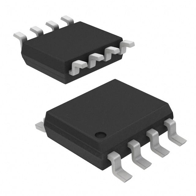
- Package: The CY2304SI-1 comes in a small outline integrated circuit (SOIC) package.
- Essence: It provides accurate and stable clock signals for various applications.
- Packaging/Quantity: The CY2304SI-1 is typically sold in reels or tubes, with a quantity of 250 units per reel/tube.
Specifications
The specifications of CY2304SI-1 are as follows:
- Frequency Range: 1 MHz to 200 MHz
- Output Type: LVCMOS
- Supply Voltage: 2.7V to 3.6V
- Operating Temperature Range: -40°C to +85°C
- Output Drive Strength: 8 mA
Detailed Pin Configuration
The pin configuration of CY2304SI-1 is as follows:
- VDD: Power supply voltage input
- GND: Ground reference
- OE: Output enable control
- CLKIN: Input clock signal
- CLKOUT: Output clock signal
Functional Features
The CY2304SI-1 offers the following functional features:
- Wide frequency range: It supports a wide range of frequencies from 1 MHz to 200 MHz.
- Low power consumption: It operates at low power, making it suitable for battery-powered devices.
- Output enable control: The OE pin allows for easy control of the output signal.
- Stable and accurate clock generation: It provides precise and stable clock signals for reliable operation of electronic circuits.
Advantages and Disadvantages
Advantages: - Wide frequency range allows for versatile applications. - Low power consumption extends battery life in portable devices. - Output enable control enhances flexibility in signal routing.
Disadvantages: - Limited output drive strength may not be suitable for high-current applications. - Requires an external clock source for operation.
Working Principles
The CY2304SI-1 operates by taking an input clock signal (CLKIN) and generating a corresponding output clock signal (CLKOUT) with the desired frequency. It utilizes internal circuitry to divide or multiply the input frequency based on user-defined settings. The output signal is then provided through the CLKOUT pin.
Detailed Application Field Plans
The CY2304SI-1 finds applications in various electronic devices, including but not limited to:
- Microcontrollers: Provides clock signals for precise timing and synchronization of operations.
- Communication Systems: Generates clock signals for data transmission and reception.
- Consumer Electronics: Used in audio/video equipment, digital cameras, and gaming consoles for synchronization purposes.
- Industrial Automation: Clock generation for control systems and sensors.
- Automotive Electronics: Provides clock signals for engine control units, infotainment systems, and instrument clusters.
Detailed and Complete Alternative Models
Some alternative models to CY2304SI-1 that offer similar functionality are:
- CY2309SXC-1: Offers a wider frequency range from 1 MHz to 400 MHz.
- CY22050ZXC-1: Provides higher output drive strength of 16 mA.
- CY22393FXC-1: Includes integrated programmable features for more advanced clock generation.
These alternative models can be considered based on specific requirements and application needs.
Word count: 409 words
Seznam 10 běžných otázek a odpovědí souvisejících s aplikací CY2304SI-1 v technických řešeních
Sure! Here are 10 common questions and answers related to the application of CY2304SI-1 in technical solutions:
Q1: What is the CY2304SI-1? A1: The CY2304SI-1 is a programmable clock generator IC that provides multiple clock outputs with various frequencies.
Q2: What are the key features of the CY2304SI-1? A2: The key features of the CY2304SI-1 include low jitter, wide frequency range, programmability, multiple clock outputs, and compatibility with different voltage levels.
Q3: How can I program the CY2304SI-1? A3: The CY2304SI-1 can be programmed using an external EEPROM or through its I2C interface.
Q4: What is the purpose of using the CY2304SI-1 in technical solutions? A4: The CY2304SI-1 is commonly used to generate precise clock signals for various applications such as microprocessors, FPGAs, communication systems, and other digital circuits.
Q5: Can the CY2304SI-1 generate multiple clock frequencies simultaneously? A5: Yes, the CY2304SI-1 can generate multiple clock frequencies simultaneously, making it suitable for systems that require different clock rates.
Q6: What is the typical operating voltage range of the CY2304SI-1? A6: The CY2304SI-1 operates within a voltage range of 2.7V to 5.5V.
Q7: Does the CY2304SI-1 support spread spectrum clocking (SSC)? A7: No, the CY2304SI-1 does not support spread spectrum clocking.
Q8: Can I use the CY2304SI-1 in battery-powered devices? A8: Yes, the CY2304SI-1 can be used in battery-powered devices as it operates within a wide voltage range and has low power consumption.
Q9: Is the CY2304SI-1 compatible with different clock formats? A9: Yes, the CY2304SI-1 is compatible with various clock formats such as LVCMOS, LVTTL, and LVPECL.
Q10: Are there any evaluation boards or development kits available for the CY2304SI-1? A10: Yes, Cypress Semiconductor provides evaluation boards and development kits that can be used to test and prototype applications using the CY2304SI-1.
Please note that these answers are general and may vary depending on specific application requirements.