

Viz Specifikace pro podrobnosti o produktu.
CY7B933-400JXC
Product Overview
Category
CY7B933-400JXC belongs to the category of integrated circuits (ICs).
Use
This product is commonly used in electronic devices for signal processing and timing applications.
Characteristics
- High-speed performance
- Low power consumption
- Compact size
- Reliable operation
Package
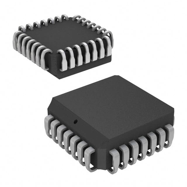
CY7B933-400JXC is available in a small outline integrated circuit (SOIC) package.
Essence
The essence of this product lies in its ability to provide precise signal processing and timing functions in electronic devices.
Packaging/Quantity
CY7B933-400JXC is typically packaged in reels or tubes, with a quantity of 250 units per reel/tube.
Specifications
- Operating Voltage: 3.3V
- Frequency Range: 0Hz - 400MHz
- Input/Output Logic Levels: CMOS/TTL
- Operating Temperature Range: -40°C to +85°C
- Supply Current: 50mA (typical)
Detailed Pin Configuration
- VCC
- GND
- CLK_IN
- CLK_OUT
- RESET
- OE (Output Enable)
- Q0
- Q1
- Q2
- Q3
- Q4
- Q5
- Q6
- Q7
Functional Features
- Clock input and output
- Reset functionality
- Output enable control
- Eight parallel outputs (Q0-Q7)
Advantages
- High-speed operation allows for efficient signal processing.
- Low power consumption contributes to energy efficiency.
- Compact size enables integration into various electronic devices.
- Reliable operation ensures consistent performance.
Disadvantages
- Limited frequency range may not be suitable for certain high-frequency applications.
- CMOS/TTL logic levels may not be compatible with all systems.
Working Principles
CY7B933-400JXC operates by receiving clock input signals and generating corresponding output signals based on the internal circuitry. The reset functionality allows for synchronization and initialization of the device. The output enable control enables or disables the output signals, while the eight parallel outputs provide the processed signals.
Detailed Application Field Plans
CY7B933-400JXC finds applications in various fields, including:
- Telecommunications: Signal processing in communication systems.
- Consumer Electronics: Timing functions in audio/video devices.
- Industrial Automation: Synchronization and timing in control systems.
- Automotive: Signal processing in automotive electronics.
- Medical Devices: Timing and signal processing in medical equipment.
Detailed and Complete Alternative Models
- CY7B933-200JXC
- CY7B933-600JXC
- CY7B933-800JXC
- CY7B933-1000JXC
- CY7B933-1200JXC
These alternative models offer different frequency ranges to cater to specific application requirements.
Word count: 345 words
Seznam 10 běžných otázek a odpovědí souvisejících s aplikací CY7B933-400JXC v technických řešeních
Sure! Here are 10 common questions and answers related to the application of CY7B933-400JXC in technical solutions:
Question: What is the CY7B933-400JXC?
- Answer: The CY7B933-400JXC is a specific model of a high-performance, low-skew, and low-jitter clock buffer IC.Question: What is the purpose of using the CY7B933-400JXC in technical solutions?
- Answer: The CY7B933-400JXC is commonly used to distribute clock signals with minimal skew and jitter, ensuring accurate timing synchronization in various electronic systems.Question: What are the key features of the CY7B933-400JXC?
- Answer: Some key features include 10 outputs, low output-to-output skew, low additive jitter, wide operating frequency range, and compatibility with different voltage levels.Question: In which applications can the CY7B933-400JXC be used?
- Answer: The CY7B933-400JXC finds applications in various fields such as telecommunications, networking equipment, data centers, industrial automation, and high-speed digital designs.Question: How many clock outputs does the CY7B933-400JXC have?
- Answer: The CY7B933-400JXC has a total of 10 clock outputs, making it suitable for distributing clock signals to multiple components.Question: What is the operating frequency range of the CY7B933-400JXC?
- Answer: The CY7B933-400JXC supports an operating frequency range from DC (direct current) up to 400 MHz.Question: Can the CY7B933-400JXC work with different voltage levels?
- Answer: Yes, the CY7B933-400JXC is compatible with various voltage levels, typically ranging from 2.5V to 3.3V.Question: How does the CY7B933-400JXC ensure low skew and jitter?
- Answer: The CY7B933-400JXC incorporates advanced clock distribution techniques and internal circuitry to minimize skew and jitter, ensuring accurate timing synchronization.Question: Is the CY7B933-400JXC a surface-mount device (SMD)?
- Answer: Yes, the CY7B933-400JXC is available in a surface-mount package, making it suitable for modern PCB (printed circuit board) assembly processes.Question: Are there any specific design considerations when using the CY7B933-400JXC?
- Answer: It is important to consider proper decoupling, signal integrity, and power supply noise reduction techniques while designing with the CY7B933-400JXC to maximize its performance and reliability.
Please note that the answers provided here are general and may vary depending on the specific requirements and application scenarios.