

Viz Specifikace pro podrobnosti o produktu.
CY7B9910-5SI
Product Overview
Category
The CY7B9910-5SI belongs to the category of integrated circuits (ICs).
Use
This IC is primarily used for clock generation and distribution in electronic devices.
Characteristics
- Clock frequency range: 1 MHz to 200 MHz
- Low jitter performance
- Wide operating voltage range: 2.7V to 3.6V
- Output skew control
- Programmable output signal format
Package
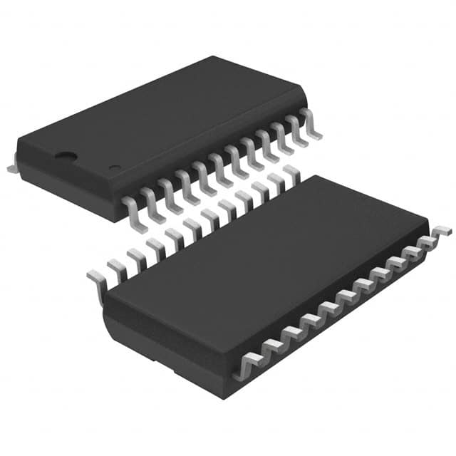
The CY7B9910-5SI is available in a small outline integrated circuit (SOIC) package.
Essence
The essence of the CY7B9910-5SI lies in its ability to generate and distribute accurate clock signals, ensuring synchronization and timing integrity in electronic systems.
Packaging/Quantity
The CY7B9910-5SI is typically packaged in reels or tubes, with a quantity of 250 units per reel/tube.
Specifications
- Supply voltage: 2.7V to 3.6V
- Operating temperature range: -40°C to +85°C
- Output frequency range: 1 MHz to 200 MHz
- Output signal formats: LVPECL, LVDS, HCSL, CML
- Output skew control range: ±500 ps
- Input reference clock frequency range: 1 MHz to 200 MHz
Detailed Pin Configuration
The CY7B9910-5SI has a total of 20 pins. The pin configuration is as follows:
- VDD
- GND
- REFCLK
- OE
- CLKOUT0
- CLKOUT1
- CLKOUT2
- CLKOUT3
- CLKOUT4
- CLKOUT5
- CLKOUT6
- CLKOUT7
- CLKOUT8
- CLKOUT9
- CLKOUT10
- CLKOUT11
- CLKOUT12
- CLKOUT13
- CLKOUT14
- CLKOUT15
Functional Features
- Clock generation and distribution: The CY7B9910-5SI can generate multiple clock signals with low jitter from a single reference clock input.
- Output skew control: It allows precise control of the relative timing between different clock outputs.
- Programmable output signal format: The IC supports various output signal formats, including LVPECL, LVDS, HCSL, and CML.
Advantages and Disadvantages
Advantages
- Wide operating voltage range enables compatibility with various systems.
- Low jitter performance ensures accurate timing synchronization.
- Output skew control allows fine-tuning of clock signals.
- Programmable output signal format provides flexibility in system integration.
Disadvantages
- Limited output frequency range (1 MHz to 200 MHz).
- Relatively complex pin configuration may require careful attention during circuit design.
Working Principles
The CY7B9910-5SI operates by taking an input reference clock and using internal phase-locked loop (PLL) circuits to generate multiple synchronized clock signals. These clock signals are then distributed to the corresponding output pins. The output skew control feature allows adjustment of the relative timing between the clock outputs.
Detailed Application Field Plans
The CY7B9910-5SI finds applications in various electronic systems that require precise clock generation and distribution. Some specific application fields include:
- Communication systems: Used for clock synchronization in network switches, routers, and communication infrastructure equipment.
- Data storage devices: Ensures accurate timing in hard disk drives, solid-state drives, and RAID systems.
- Industrial automation: Provides synchronized clock signals for PLCs (Programmable Logic Controllers) and industrial control systems.
- Test and measurement equipment: Used in oscilloscopes, signal generators, and other test instruments to maintain accurate timing.
Detailed and Complete Alternative Models
- CY7B9910-5SX: Similar to CY7B9910-5SI, but available in a different package (SOT-23).
- CY7B9910-5SC: Offers the same functionality as CY7B9910-5SI, but with extended temperature range (-40°C to +125°C).
- CY7B9910-5SPC: Provides additional features such as frequency multiplication/division and programmable delay.
These alternative models offer similar clock generation and distribution capabilities, catering to different packaging requirements or specific application needs.
Word count: 550 words
Seznam 10 běžných otázek a odpovědí souvisejících s aplikací CY7B9910-5SI v technických řešeních
Sure! Here are 10 common questions and answers related to the application of CY7B9910-5SI in technical solutions:
Question: What is the CY7B9910-5SI?
Answer: The CY7B9910-5SI is a high-performance, low-skew, low-jitter clock buffer designed for use in various electronic systems.Question: What is the purpose of using the CY7B9910-5SI in a technical solution?
Answer: The CY7B9910-5SI is used to distribute clock signals with minimal skew and jitter, ensuring accurate timing synchronization in complex digital systems.Question: What are the key features of the CY7B9910-5SI?
Answer: Some key features include low output skew, low additive jitter, wide operating frequency range, and multiple outputs for signal distribution.Question: In which applications can the CY7B9910-5SI be used?
Answer: The CY7B9910-5SI is commonly used in telecommunications, networking equipment, data centers, and other high-speed digital systems that require precise clock distribution.Question: How many outputs does the CY7B9910-5SI have?
Answer: The CY7B9910-5SI has 10 outputs, allowing it to distribute clock signals to multiple components or subsystems.Question: What is the maximum operating frequency of the CY7B9910-5SI?
Answer: The CY7B9910-5SI can operate at frequencies up to 200 MHz, making it suitable for a wide range of high-speed applications.Question: Does the CY7B9910-5SI support different voltage levels?
Answer: Yes, the CY7B9910-5SI supports both 3.3V and 2.5V voltage levels, providing flexibility in system design.Question: Can the CY7B9910-5SI be cascaded with other clock buffers?
Answer: Yes, the CY7B9910-5SI can be cascaded with other clock buffers to expand the number of outputs or improve signal integrity.Question: How does the CY7B9910-5SI handle input clock signals?
Answer: The CY7B9910-5SI has differential inputs that accept LVPECL, LVDS, or CML input signals, allowing compatibility with various clock sources.Question: Is the CY7B9910-5SI available in different package options?
Answer: Yes, the CY7B9910-5SI is available in a small-outline integrated circuit (SOIC) package, making it easy to integrate into different PCB designs.
Please note that these questions and answers are for illustrative purposes and may vary depending on specific application requirements.