

Viz Specifikace pro podrobnosti o produktu.
CY7C025-25JXI
Product Overview
Category
CY7C025-25JXI belongs to the category of integrated circuits (ICs).
Use
This product is commonly used in electronic devices for various applications such as data storage, signal processing, and control systems.
Characteristics
- High-speed performance
- Low power consumption
- Compact size
- Reliable operation
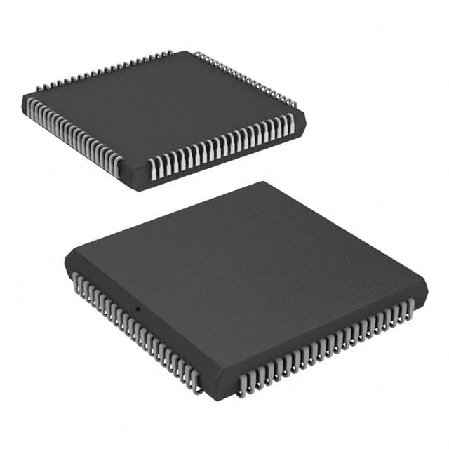
Package
CY7C025-25JXI is available in a small outline integrated circuit (SOIC) package.
Essence
The essence of CY7C025-25JXI lies in its ability to provide efficient and reliable data processing and storage capabilities within electronic devices.
Packaging/Quantity
CY7C025-25JXI is typically packaged in reels or tubes, with each reel or tube containing a specific quantity of ICs. The exact packaging and quantity may vary depending on the manufacturer.
Specifications
- Operating Voltage: 3.3V
- Speed Grade: 25 ns
- Memory Size: 256 kilobits (32 kilobytes)
- Organization: 32K x 8 bits
- Interface: Parallel
- Operating Temperature Range: -40°C to +85°C
Detailed Pin Configuration
The pin configuration of CY7C025-25JXI is as follows:
- VCC
- A0
- A1
- A2
- A3
- A4
- A5
- A6
- A7
- CE#
- OE#
- WE#
- I/O0
- I/O1
- I/O2
- I/O3
- I/O4
- I/O5
- I/O6
- I/O7
- GND
Functional Features
- High-speed access and data transfer
- Low power consumption during standby mode
- Easy integration into existing electronic systems
- Reliable performance in various operating conditions
Advantages and Disadvantages
Advantages
- Fast data processing and storage capabilities
- Compact size allows for space-efficient designs
- Low power consumption helps prolong battery life in portable devices
- Wide operating temperature range enables usage in extreme environments
Disadvantages
- Limited memory size compared to higher-capacity ICs
- Parallel interface may not be suitable for all applications
- Higher cost compared to lower-end ICs with similar functionality
Working Principles
CY7C025-25JXI operates based on the principles of digital logic and memory storage. It uses a parallel interface to communicate with the host device, allowing for fast data transfer between the IC and other components.
Detailed Application Field Plans
CY7C025-25JXI finds applications in various fields, including but not limited to: 1. Consumer electronics: Used in smartphones, tablets, and digital cameras for data storage and processing. 2. Industrial automation: Integrated into control systems for efficient data handling and real-time processing. 3. Automotive electronics: Utilized in vehicle control units for reliable and high-speed data transfer. 4. Medical devices: Incorporated into medical equipment for data storage and signal processing.
Detailed and Complete Alternative Models
Some alternative models that offer similar functionality to CY7C025-25JXI are: 1. CY7C026-20AXI 2. CY7C027-15AC 3. CY7C028V-15AXC 4. CY7C029V-20AI
These models provide comparable features and can be considered as alternatives depending on specific requirements and compatibility with the target application.
Word count: 520 words
Seznam 10 běžných otázek a odpovědí souvisejících s aplikací CY7C025-25JXI v technických řešeních
Sure! Here are 10 common questions and answers related to the application of CY7C025-25JXI in technical solutions:
Question: What is the CY7C025-25JXI?
Answer: The CY7C025-25JXI is a specific model of a high-speed asynchronous static RAM (SRAM) chip.Question: What is the maximum operating frequency of the CY7C025-25JXI?
Answer: The CY7C025-25JXI can operate at a maximum frequency of 25 MHz.Question: What is the storage capacity of the CY7C025-25JXI?
Answer: The CY7C025-25JXI has a storage capacity of 256 kilobits (32 kilobytes).Question: What voltage levels does the CY7C025-25JXI support?
Answer: The CY7C025-25JXI supports a single power supply voltage of 5V.Question: Can the CY7C025-25JXI be used in battery-powered devices?
Answer: No, the CY7C025-25JXI is not suitable for battery-powered devices due to its higher power consumption.Question: What is the access time of the CY7C025-25JXI?
Answer: The CY7C025-25JXI has an access time of 25 ns, which refers to the time it takes to read or write data.Question: Is the CY7C025-25JXI compatible with other SRAM chips?
Answer: Yes, the CY7C025-25JXI follows industry-standard pinout and timing specifications, making it compatible with other SRAM chips.Question: Can the CY7C025-25JXI be used in industrial applications?
Answer: Yes, the CY7C025-25JXI is suitable for various industrial applications that require high-speed and reliable data storage.Question: Does the CY7C025-25JXI have any built-in error correction capabilities?
Answer: No, the CY7C025-25JXI does not have built-in error correction capabilities. Additional error correction mechanisms may need to be implemented if required.Question: What is the package type of the CY7C025-25JXI?
Answer: The CY7C025-25JXI comes in a 32-pin plastic J-lead chip carrier (PLCC) package.
Please note that these answers are based on general information about the CY7C025-25JXI and may vary depending on specific application requirements.