

Viz Specifikace pro podrobnosti o produktu.
CY7C1041CV33-20VXE
Product Overview
Category
The CY7C1041CV33-20VXE belongs to the category of integrated circuits (ICs), specifically a synchronous static random access memory (SRAM) chip.
Use
This IC is primarily used as a high-speed, low-power memory solution in various electronic devices and systems. It provides fast and reliable data storage and retrieval capabilities.
Characteristics
- High-speed operation: The CY7C1041CV33-20VXE offers fast access times, allowing for efficient data processing.
- Low power consumption: This IC is designed to minimize power usage, making it suitable for battery-powered devices.
- Large storage capacity: With a capacity of 4 megabits (512K x 8 bits), it can store a significant amount of data.
- Synchronous interface: The chip operates synchronously with the system clock, enabling precise timing control.
Package
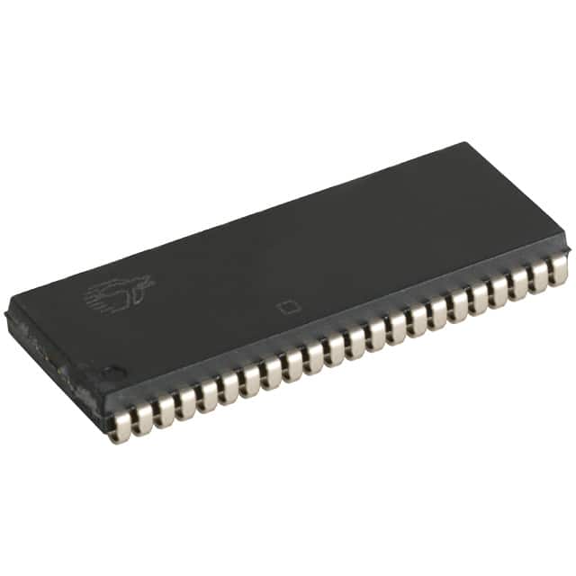
The CY7C1041CV33-20VXE is available in a compact and industry-standard 44-pin TSOP (Thin Small Outline Package). This package ensures easy integration into circuit boards and facilitates efficient heat dissipation.
Essence
The essence of the CY7C1041CV33-20VXE lies in its ability to provide high-speed and low-power memory functionality, enhancing the overall performance of electronic devices.
Packaging/Quantity
The CY7C1041CV33-20VXE is typically packaged in reels or tubes, containing multiple units per package. The exact quantity may vary depending on the supplier and customer requirements.
Specifications
- Organization: 512K x 8 bits
- Operating Voltage: 3.3V ± 0.3V
- Access Time: 20 ns (max)
- Standby Current: 10 μA (typical)
- Operating Temperature Range: -40°C to +85°C
- Data Retention Voltage: 2.0V (min)
Detailed Pin Configuration
The CY7C1041CV33-20VXE features a total of 44 pins, each serving a specific purpose. The pin configuration is as follows:
- A0-A18: Address Inputs
- DQ0-DQ7: Data Input/Output
- WE#: Write Enable
- OE#: Output Enable
- CE#: Chip Enable
- UB#/LB#: Upper/Lower Byte Control
- VCC: Power Supply
- GND: Ground
(Note: The remaining pin details can be found in the product datasheet.)
Functional Features
- High-speed operation: The CY7C1041CV33-20VXE offers fast access times, enabling quick data retrieval and processing.
- Low power consumption: This IC is designed to minimize power usage, making it suitable for energy-efficient devices.
- Easy integration: The industry-standard package and pin configuration facilitate seamless integration into various circuit designs.
- Reliable data storage: The chip ensures reliable data retention, even in challenging environmental conditions.
Advantages and Disadvantages
Advantages
- Fast access times enhance overall system performance.
- Low power consumption prolongs battery life in portable devices.
- Large storage capacity accommodates extensive data requirements.
- Synchronous interface allows precise timing control.
Disadvantages
- Limited compatibility with certain legacy systems that require different voltage levels or interfaces.
- Relatively higher cost compared to alternative memory solutions with lower specifications.
Working Principles
The CY7C1041CV33-20VXE operates based on the principles of synchronous static random access memory (SRAM). It stores data in a volatile manner, meaning that the stored information is lost when power is removed. The chip utilizes an address bus to select specific memory locations and a data bus for reading from or writing to those locations. The synchronous interface ensures that data transfers occur in synchronization with the system clock, enabling precise timing control.
Detailed Application Field Plans
The CY7C1041CV33-20VXE finds applications in various electronic devices and systems, including but not limited to: - Computer systems - Networking equipment - Telecommunications devices - Consumer electronics - Industrial automation systems
In computer systems, this IC can be used as cache memory or as part of the main memory subsystem. In networking and telecommunications equipment, it enables fast data buffering and storage. In consumer electronics, it supports high-speed data processing in devices such as digital cameras and gaming consoles. In industrial automation systems, it provides reliable memory storage for critical data.
Detailed and Complete Alternative Models
There are several alternative models available in the market that offer similar functionality to the CY7C1041CV33-20VXE. Some notable alternatives include: - MT45W8MW16BGX-701 IT: 4Mb Synchronous SRAM, 3.3V, 20 ns access
Seznam 10 běžných otázek a odpovědí souvisejících s aplikací CY7C1041CV33-20VXE v technických řešeních
Sure! Here are 10 common questions and answers related to the application of CY7C1041CV33-20VXE in technical solutions:
Q1: What is CY7C1041CV33-20VXE? A1: CY7C1041CV33-20VXE is a specific model of synchronous SRAM (Static Random Access Memory) manufactured by Cypress Semiconductor. It has a capacity of 4 Megabits (512K x 8) and operates at a voltage of 3.3V.
Q2: What are the key features of CY7C1041CV33-20VXE? A2: Some key features of CY7C1041CV33-20VXE include a fast access time of 20 ns, low power consumption, high-speed clock operation, and compatibility with various microcontrollers and digital systems.
Q3: What are the typical applications of CY7C1041CV33-20VXE? A3: CY7C1041CV33-20VXE is commonly used in applications such as networking equipment, telecommunications devices, industrial automation systems, medical instruments, and other electronic devices that require high-speed and reliable memory storage.
Q4: How does CY7C1041CV33-20VXE connect to a microcontroller or digital system? A4: CY7C1041CV33-20VXE connects to a microcontroller or digital system using standard parallel interface connections. It requires address lines, data lines, control signals (such as chip enable and write enable), and power supply connections.
Q5: Can CY7C1041CV33-20VXE operate at different voltages? A5: No, CY7C1041CV33-20VXE operates specifically at a voltage of 3.3V. It is important to ensure that the power supply voltage matches the required operating voltage of the SRAM.
Q6: What is the maximum operating frequency of CY7C1041CV33-20VXE? A6: The maximum operating frequency of CY7C1041CV33-20VXE is typically specified by the manufacturer and depends on various factors such as temperature, voltage, and load conditions. It is important to refer to the datasheet for accurate information.
Q7: Can CY7C1041CV33-20VXE be used in battery-powered devices? A7: Yes, CY7C1041CV33-20VXE has low power consumption characteristics, making it suitable for use in battery-powered devices where energy efficiency is crucial.
Q8: Is CY7C1041CV33-20VXE compatible with other memory devices? A8: CY7C1041CV33-20VXE is compatible with other synchronous SRAM devices that have similar voltage requirements and interface specifications. However, compatibility with specific memory devices should be verified through their respective datasheets.
Q9: Can CY7C1041CV33-20VXE be used in high-temperature environments? A9: CY7C1041CV33-20VXE has a specified operating temperature range provided by the manufacturer. It is important to ensure that the device is within its specified temperature limits to maintain proper functionality.
Q10: Are there any special considerations when designing with CY7C1041CV33-20VXE? A10: When designing with CY7C1041CV33-20VXE, it is important to consider factors such as signal integrity, power supply stability, decoupling capacitors, and proper timing constraints to ensure reliable operation. Referring to the datasheet and application notes provided by the manufacturer is highly recommended.