

Viz Specifikace pro podrobnosti o produktu.
CY7C1041DV33-10ZSXIT
Product Overview
Category
The CY7C1041DV33-10ZSXIT belongs to the category of semiconductor devices.
Use
This product is primarily used in electronic circuits for data storage and retrieval purposes.
Characteristics
- High-speed operation
- Low power consumption
- Small form factor
- Reliable performance
Package
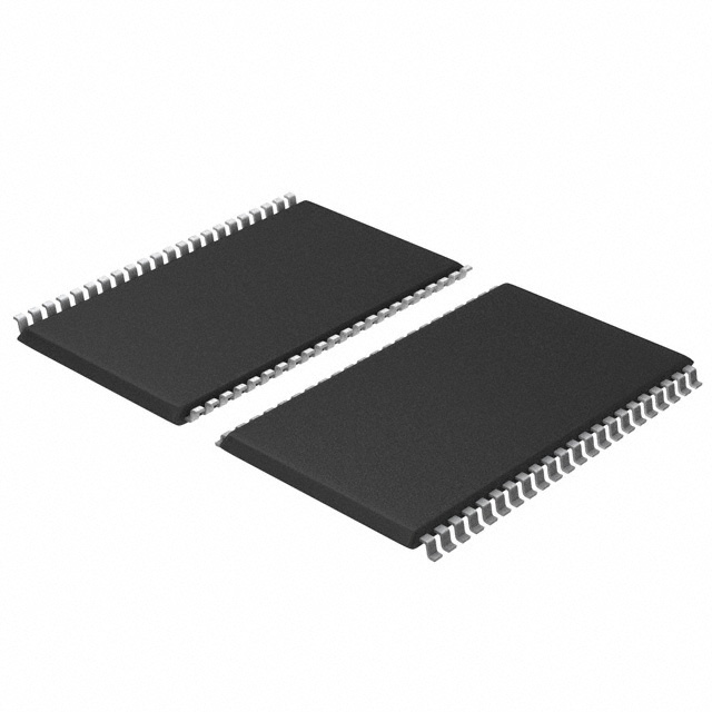
The CY7C1041DV33-10ZSXIT is available in a compact surface mount package.
Essence
The essence of this product lies in its ability to store and retrieve digital information quickly and efficiently.
Packaging/Quantity
The CY7C1041DV33-10ZSXIT is typically packaged in reels or trays, with a quantity of 2500 units per reel/tray.
Specifications
- Operating Voltage: 3.3V
- Access Time: 10ns
- Capacity: 1 Megabit (128K x 8)
- Organization: 128K words x 8 bits
- Interface: Parallel
- Operating Temperature Range: -40°C to +85°C
Detailed Pin Configuration
The CY7C1041DV33-10ZSXIT has a total of 32 pins, which are configured as follows:
- A0
- A1
- A2
- A3
- A4
- A5
- A6
- A7
- VCC
- OE#
- CE#
- WE#
- I/O0
- I/O1
- I/O2
- I/O3
- I/O4
- I/O5
- I/O6
- I/O7
- GND
- NC
- NC
- NC
- NC
- NC
- NC
- NC
- NC
- NC
- NC
- NC
Functional Features
- High-speed data access
- Low power consumption
- Easy integration into existing circuits
- Reliable performance in various operating conditions
Advantages and Disadvantages
Advantages
- Fast data access time
- Low power consumption
- Compact form factor
- Reliable performance
Disadvantages
- Limited storage capacity compared to newer memory technologies
- Parallel interface may limit compatibility with certain systems
Working Principles
The CY7C1041DV33-10ZSXIT operates based on the principles of semiconductor memory technology. It utilizes a parallel interface to transfer data between the memory cells and the external circuitry. When accessed, the memory cells retrieve or store digital information based on the control signals received.
Detailed Application Field Plans
The CY7C1041DV33-10ZSXIT finds applications in various electronic devices and systems, including but not limited to: - Computer motherboards - Networking equipment - Industrial control systems - Automotive electronics - Consumer electronics
Detailed and Complete Alternative Models
- CY7C1041DV33-10ZSXI
- CY7C1041DV33-10ZSXE
- CY7C1041DV33-10ZSXA
- CY7C1041DV33-10ZSXB
- CY7C1041DV33-10ZSXC
These alternative models offer similar specifications and functionality to the CY7C1041DV33-10ZSXIT, providing options for different application requirements.
In conclusion, the CY7C1041DV33-10ZSXIT is a high-speed, low-power semiconductor device used for data storage and retrieval. Its compact form factor, reliable performance, and easy integration make it suitable for various electronic applications. However, its limited storage capacity and parallel interface may pose limitations in certain scenarios.
Seznam 10 běžných otázek a odpovědí souvisejících s aplikací CY7C1041DV33-10ZSXIT v technických řešeních
Sure! Here are 10 common questions and answers related to the application of CY7C1041DV33-10ZSXIT in technical solutions:
Q1: What is the CY7C1041DV33-10ZSXIT? A1: The CY7C1041DV33-10ZSXIT is a high-speed, low-power, 4-megabit (256K x 16) CMOS static RAM (SRAM) device.
Q2: What is the operating voltage range for CY7C1041DV33-10ZSXIT? A2: The operating voltage range for CY7C1041DV33-10ZSXIT is 3.0V to 3.6V.
Q3: What is the maximum clock frequency supported by CY7C1041DV33-10ZSXIT? A3: The maximum clock frequency supported by CY7C1041DV33-10ZSXIT is 100 MHz.
Q4: Can CY7C1041DV33-10ZSXIT be used in battery-powered devices? A4: Yes, CY7C1041DV33-10ZSXIT is suitable for battery-powered devices due to its low power consumption.
Q5: What is the access time of CY7C1041DV33-10ZSXIT? A5: The access time of CY7C1041DV33-10ZSXIT is 10 ns.
Q6: Does CY7C1041DV33-10ZSXIT support multiple read/write operations simultaneously? A6: No, CY7C1041DV33-10ZSXIT does not support multiple read/write operations simultaneously.
Q7: Can CY7C1041DV33-10ZSXIT be used in industrial temperature environments? A7: Yes, CY7C1041DV33-10ZSXIT is designed to operate in industrial temperature ranges (-40°C to +85°C).
Q8: What is the package type for CY7C1041DV33-10ZSXIT? A8: CY7C1041DV33-10ZSXIT comes in a 48-pin TSOP-II (Thin Small Outline Package) form factor.
Q9: Is CY7C1041DV33-10ZSXIT compatible with other SRAM devices? A9: Yes, CY7C1041DV33-10ZSXIT is compatible with other standard SRAM devices and can be used as a drop-in replacement.
Q10: Can CY7C1041DV33-10ZSXIT be used in high-speed data buffering applications? A10: Yes, CY7C1041DV33-10ZSXIT is suitable for high-speed data buffering due to its fast access time and high clock frequency support.
Please note that these answers are based on general information about the CY7C1041DV33-10ZSXIT. For specific technical details and application requirements, it is recommended to refer to the datasheet or consult the manufacturer's documentation.