

Viz Specifikace pro podrobnosti o produktu.
CY7C1061DV33-10BV1XI
Product Overview
Category
CY7C1061DV33-10BV1XI belongs to the category of high-speed synchronous static random access memory (SRAM) chips.
Use
This product is commonly used in various electronic devices and systems that require fast and reliable data storage and retrieval.
Characteristics
- High-speed operation: CY7C1061DV33-10BV1XI offers fast access times, making it suitable for applications that demand quick data processing.
- Low power consumption: This SRAM chip is designed to minimize power consumption, making it energy-efficient.
- Wide temperature range: It can operate reliably across a wide temperature range, making it suitable for use in different environments.
- High density: The CY7C1061DV33-10BV1XI has a high storage capacity, allowing it to store large amounts of data.
Package
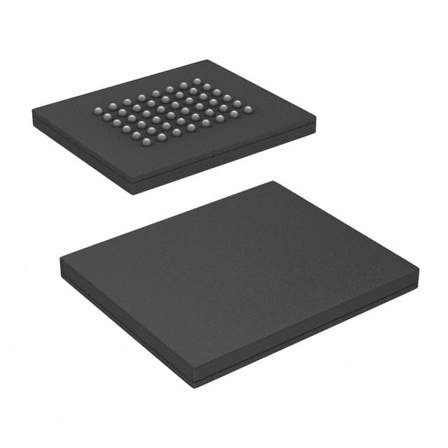
The CY7C1061DV33-10BV1XI is available in a compact and industry-standard 44-pin TSOP-II package.
Essence
This SRAM chip is an essential component in electronic devices, providing temporary storage for data during processing.
Packaging/Quantity
The CY7C1061DV33-10BV1XI is typically packaged in reels or trays, with quantities varying based on customer requirements.
Specifications
- Organization: 64K words x 16 bits
- Voltage Supply: 3.3V
- Access Time: 10ns
- Operating Temperature Range: -40°C to +85°C
- Standby Current: 5mA (max)
- Active Current: 70mA (max)
Detailed Pin Configuration
The CY7C1061DV33-10BV1XI has a total of 44 pins. Here is a detailed pin configuration:
- A0-A15: Address Inputs
- DQ0-DQ15: Data Input/Output
- WE: Write Enable
- OE: Output Enable
- CE1, CE2: Chip Enables
- UB, LB: Byte Enables
- VCC: Power Supply (3.3V)
- GND: Ground
Functional Features
- Fast Read and Write Operations: The CY7C1061DV33-10BV1XI offers high-speed data access, enabling efficient read and write operations.
- Easy Integration: This SRAM chip can be easily integrated into various electronic systems due to its standard pin configuration and compatibility.
- Low Power Consumption: With its low power consumption design, the CY7C1061DV33-10BV1XI helps conserve energy in electronic devices.
- Reliable Performance: It provides reliable performance even in harsh operating conditions, ensuring data integrity.
Advantages and Disadvantages
Advantages
- High-speed operation for quick data processing
- Low power consumption for energy efficiency
- Wide temperature range for versatile applications
- High storage capacity for large data requirements
Disadvantages
- Relatively higher cost compared to other memory technologies
- Limited availability in certain markets
Working Principles
The CY7C1061DV33-10BV1XI operates based on the synchronous static random access memory (SRAM) technology. It stores data in a volatile manner, meaning that the stored information is lost when power is removed. The chip uses an address bus to specify the location of data and a data bus to read from or write to the memory cells. The control signals such as write enable (WE), output enable (OE), and chip enables (CE1, CE2) facilitate the data transfer process.
Detailed Application Field Plans
The CY7C1061DV33-10BV1XI finds application in various electronic systems, including but not limited to: - Computer systems - Networking equipment - Communication devices - Industrial automation systems - Automotive electronics
Detailed and Complete Alternative Models
- CY7C1061DV33-10BAXI: Similar specifications, different package (48-pin TSOP-II)
- CY7C1061DV33-10BGI: Similar specifications, different package (54-ball VFBGA)
- CY7C1061DV33-10BGXI: Similar specifications, different package (54-ball VFBGA)
These alternative models offer similar functionality and performance, providing options for different system requirements.
Word count: 550 words
Seznam 10 běžných otázek a odpovědí souvisejících s aplikací CY7C1061DV33-10BV1XI v technických řešeních
Sure! Here are 10 common questions and answers related to the application of CY7C1061DV33-10BV1XI in technical solutions:
Q1: What is CY7C1061DV33-10BV1XI? A1: CY7C1061DV33-10BV1XI is a specific model of synchronous SRAM (Static Random Access Memory) chip manufactured by Cypress Semiconductor.
Q2: What is the voltage rating of CY7C1061DV33-10BV1XI? A2: The voltage rating of CY7C1061DV33-10BV1XI is 3.3V.
Q3: What is the capacity of CY7C1061DV33-10BV1XI? A3: CY7C1061DV33-10BV1XI has a capacity of 1 Megabit (128K x 8 bits).
Q4: What is the operating speed of CY7C1061DV33-10BV1XI? A4: CY7C1061DV33-10BV1XI operates at a speed of 10 nanoseconds (ns).
Q5: What are some typical applications of CY7C1061DV33-10BV1XI? A5: CY7C1061DV33-10BV1XI is commonly used in various technical solutions such as embedded systems, networking equipment, telecommunications devices, and industrial control systems.
Q6: Does CY7C1061DV33-10BV1XI support multiple read/write operations simultaneously? A6: No, CY7C1061DV33-10BV1XI does not support simultaneous multiple read/write operations. It operates in a single-read/single-write mode.
Q7: Can CY7C1061DV33-10BV1XI operate at different voltage levels? A7: No, CY7C1061DV33-10BV1XI operates only at a fixed voltage level of 3.3V.
Q8: Is CY7C1061DV33-10BV1XI compatible with other SRAM chips? A8: Yes, CY7C1061DV33-10BV1XI is compatible with other SRAM chips that have similar specifications and interface requirements.
Q9: Does CY7C1061DV33-10BV1XI have any built-in error correction mechanisms? A9: No, CY7C1061DV33-10BV1XI does not have built-in error correction mechanisms. It is a standard synchronous SRAM chip.
Q10: Can CY7C1061DV33-10BV1XI be used in low-power applications? A10: Yes, CY7C1061DV33-10BV1XI has low-power standby and power-down modes, making it suitable for low-power applications where energy efficiency is important.
Please note that these answers are general and may vary depending on the specific requirements and use cases.