

Viz Specifikace pro podrobnosti o produktu.
CY7C144-15JXI
Product Overview
Category
CY7C144-15JXI belongs to the category of integrated circuits (ICs).
Use
This product is commonly used in electronic devices for various applications such as data storage, signal processing, and control systems.
Characteristics
- High-speed performance
- Low power consumption
- Compact size
- Reliable operation
- Wide operating temperature range
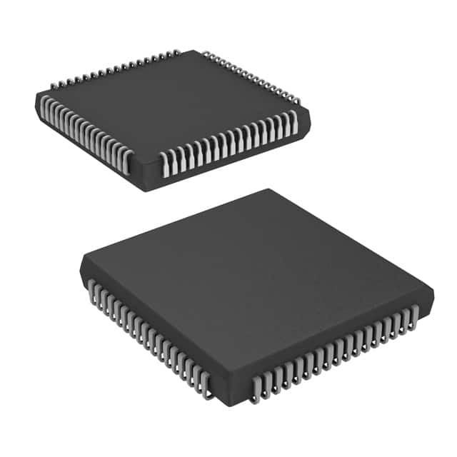
Package
CY7C144-15JXI is available in a small outline integrated circuit (SOIC) package. This package provides ease of handling and compatibility with standard PCB manufacturing processes.
Essence
The essence of CY7C144-15JXI lies in its ability to provide efficient and reliable digital data storage and processing capabilities within a compact form factor.
Packaging/Quantity
CY7C144-15JXI is typically packaged in reels or tubes, containing a specific quantity of ICs per package. The exact packaging and quantity may vary depending on the manufacturer and supplier.
Specifications
- Operating Voltage: 3.3V
- Speed Grade: 15ns
- Memory Size: 4K x 4 bits
- Interface: Parallel
- Operating Temperature Range: -40°C to +85°C
- Package Type: SOIC
Detailed Pin Configuration
The pin configuration of CY7C144-15JXI is as follows:
- VCC
- A0
- A1
- A2
- A3
- CE
- OE
- WE
- I/O0
- I/O1
- I/O2
- I/O3
- GND
Functional Features
- Random access memory (RAM) functionality
- High-speed read and write operations
- Easy interfacing with microcontrollers and other digital devices
- Low power standby mode for energy efficiency
- Chip enable and output enable control for efficient data transfer
Advantages and Disadvantages
Advantages
- High-speed performance allows for quick data access and processing.
- Low power consumption helps in reducing overall energy usage.
- Compact size enables integration into space-constrained electronic devices.
- Reliable operation ensures consistent performance over extended periods.
- Wide operating temperature range makes it suitable for various environments.
Disadvantages
- Limited memory size may not be sufficient for certain applications requiring larger storage capacity.
- Parallel interface may not be compatible with all modern digital systems that primarily use serial interfaces.
Working Principles
CY7C144-15JXI operates based on the principles of random access memory (RAM). It stores and retrieves digital data using an address-based system. The chip enable (CE), output enable (OE), and write enable (WE) pins control the read and write operations, allowing efficient data transfer between the IC and external devices.
Detailed Application Field Plans
CY7C144-15JXI finds applications in various fields, including but not limited to: - Embedded systems - Industrial automation - Communication equipment - Consumer electronics - Automotive electronics
Detailed and Complete Alternative Models
Some alternative models that offer similar functionality to CY7C144-15JXI are: - CY7C145-15AXI - CY7C146-15JXC - CY7C147-15VC
These models provide comparable specifications and features, making them suitable alternatives for different design requirements.
Word count: 410 words
Seznam 10 běžných otázek a odpovědí souvisejících s aplikací CY7C144-15JXI v technických řešeních
Sure! Here are 10 common questions and answers related to the application of CY7C144-15JXI in technical solutions:
Q: What is the CY7C144-15JXI? A: The CY7C144-15JXI is a high-speed, low-power CMOS static RAM (SRAM) with a capacity of 4K x 4 bits.
Q: What are the key features of CY7C144-15JXI? A: Some key features include a fast access time of 15 ns, low power consumption, wide operating voltage range, and compatibility with various microcontrollers and processors.
Q: What are the typical applications of CY7C144-15JXI? A: CY7C144-15JXI is commonly used in embedded systems, industrial automation, telecommunications equipment, networking devices, and other applications that require fast and reliable data storage.
Q: How do I interface CY7C144-15JXI with a microcontroller or processor? A: CY7C144-15JXI uses a parallel interface, so you can connect it to the address, data, and control lines of your microcontroller or processor.
Q: What is the operating voltage range for CY7C144-15JXI? A: CY7C144-15JXI operates within a voltage range of 4.5V to 5.5V.
Q: Can I use CY7C144-15JXI in battery-powered devices? A: Yes, CY7C144-15JXI has low power consumption, making it suitable for battery-powered devices where power efficiency is crucial.
Q: Does CY7C144-15JXI support multiple read/write operations simultaneously? A: No, CY7C144-15JXI is a synchronous SRAM and can only perform one read or write operation at a time.
Q: What is the maximum operating temperature for CY7C144-15JXI? A: The maximum operating temperature for CY7C144-15JXI is typically 70°C.
Q: Can I use CY7C144-15JXI in high-speed applications? A: Yes, CY7C144-15JXI has a fast access time of 15 ns, making it suitable for high-speed applications that require quick data retrieval.
Q: Are there any specific precautions to consider when using CY7C144-15JXI? A: It is important to follow the recommended operating conditions, handle the device properly to avoid electrostatic discharge (ESD), and ensure proper decoupling and power supply stability for reliable operation.
Please note that these answers are general and may vary depending on the specific requirements and application context.