

Viz Specifikace pro podrobnosti o produktu.
S25FL064P0XNFI000
Product Overview
- Category: Flash Memory
- Use: Data storage and retrieval in electronic devices
- Characteristics:
- Non-volatile memory
- High-speed read and write operations
- Low power consumption
- Wide temperature range (-40°C to +85°C)
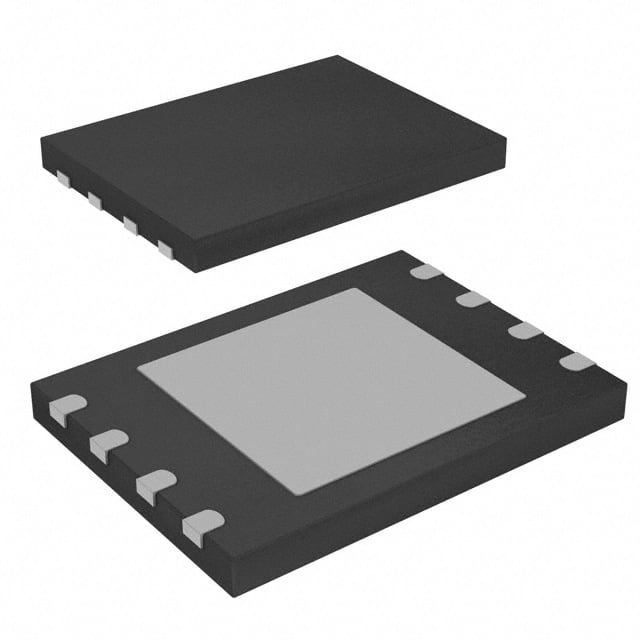
- Package: 8-pin SOIC (Small Outline Integrated Circuit)
- Essence: Reliable and efficient flash memory solution
- Packaging/Quantity: Available in tape and reel packaging, quantity varies based on customer requirements
Specifications
- Memory Capacity: 64 Megabits (8 Megabytes)
- Interface: Serial Peripheral Interface (SPI)
- Operating Voltage: 2.7V to 3.6V
- Operating Frequency: Up to 104 MHz
- Page Size: 256 bytes
- Erase Sector Size: 4 kilobytes
- Write Endurance: 100,000 cycles per sector
- Data Retention: 20 years
Pin Configuration
The S25FL064P0XNFI000 has the following pin configuration:
- Chip Select (/CS)
- Serial Clock (SCLK)
- Serial Data Input (SI)
- Serial Data Output (SO)
- Write Protect (/WP)
- Hold (/HOLD)
- Ground (GND)
- Power Supply (VCC)
Functional Features
- High-speed data transfer with SPI interface
- Efficient sector-based erase and write operations
- Hardware and software protection mechanisms
- Flexible power management options
- Support for multiple read and write modes
Advantages
- Fast read and write operations enable quick data access
- Low power consumption extends battery life in portable devices
- Wide temperature range allows usage in various environments
- Reliable data retention ensures long-term storage integrity
Disadvantages
- Limited storage capacity compared to higher-capacity flash memory options
- Higher cost per megabyte compared to larger capacity alternatives
Working Principles
The S25FL064P0XNFI000 utilizes the Serial Peripheral Interface (SPI) for communication with the host device. It stores data in non-volatile memory cells, which retain information even when power is removed. The SPI interface allows for high-speed data transfer between the flash memory and the host device.
Detailed Application Field Plans
The S25FL064P0XNFI000 is commonly used in various electronic devices, including:
- Consumer electronics (e.g., smartphones, tablets, digital cameras)
- Automotive systems (e.g., infotainment systems, instrument clusters)
- Industrial equipment (e.g., control systems, data loggers)
- Networking devices (e.g., routers, switches)
- Medical devices (e.g., patient monitors, diagnostic equipment)
Alternative Models
Other flash memory models that can be considered as alternatives to the S25FL064P0XNFI000 include:
- S25FL032P0XNFI000 - 32 Megabit (4 Megabyte) capacity
- S25FL128P0XNFI001 - 128 Megabit (16 Megabyte) capacity
- S25FL256SAGMFI010 - 256 Megabit (32 Megabyte) capacity
These alternative models offer different storage capacities to suit specific application requirements.
Word count: 346 words
Seznam 10 běžných otázek a odpovědí souvisejících s aplikací S25FL064P0XNFI000 v technických řešeních
Sure! Here are 10 common questions and answers related to the application of S25FL064P0XNFI000 in technical solutions:
Q: What is the S25FL064P0XNFI000? A: The S25FL064P0XNFI000 is a serial NOR flash memory chip manufactured by Cypress Semiconductor. It has a capacity of 64 megabits (8 megabytes) and operates on a Serial Peripheral Interface (SPI).
Q: What are the typical applications of S25FL064P0XNFI000? A: The S25FL064P0XNFI000 is commonly used in various embedded systems, such as automotive electronics, industrial control systems, consumer electronics, and networking equipment.
Q: What voltage does the S25FL064P0XNFI000 operate at? A: The S25FL064P0XNFI000 operates at a supply voltage of 2.7V to 3.6V.
Q: What is the maximum data transfer rate of the S25FL064P0XNFI000? A: The S25FL064P0XNFI000 supports a maximum clock frequency of 104 MHz, allowing for fast data transfer rates.
Q: Can the S25FL064P0XNFI000 be easily integrated into existing designs? A: Yes, the S25FL064P0XNFI000 is designed to be pin-compatible with other popular serial flash memory chips, making it relatively easy to replace or upgrade existing designs.
Q: Does the S25FL064P0XNFI000 support hardware and software protection features? A: Yes, the S25FL064P0XNFI000 provides hardware and software protection mechanisms, such as write protection, block protection, and password protection, to secure the stored data.
Q: What is the typical endurance of the S25FL064P0XNFI000? A: The S25FL064P0XNFI000 has a typical endurance of 100,000 program/erase cycles per sector, ensuring reliable and long-lasting data storage.
Q: Can the S25FL064P0XNFI000 operate in extreme temperature conditions? A: Yes, the S25FL064P0XNFI000 is designed to operate reliably in a wide temperature range, typically from -40°C to +85°C.
Q: Does the S25FL064P0XNFI000 support over-the-air (OTA) firmware updates? A: Yes, the S25FL064P0XNFI000 can be used for OTA firmware updates in devices that require remote software upgrades.
Q: Are there any development tools or software libraries available for working with the S25FL064P0XNFI000? A: Yes, Cypress Semiconductor provides various development tools, software libraries, and documentation to assist developers in integrating and programming the S25FL064P0XNFI000 in their applications.
Please note that the answers provided here are general and may vary depending on specific implementation details and requirements.