

Viz Specifikace pro podrobnosti o produktu.
S29GL01GP11FAIR12
Product Overview
- Category: Flash Memory
- Use: Data storage and retrieval in electronic devices
- Characteristics: High capacity, non-volatile, fast read/write speeds
- Package: Integrated circuit (IC) chip
- Essence: Non-volatile memory technology for long-term data storage
- Packaging/Quantity: Typically sold in trays or reels containing multiple chips
Specifications
- Memory Capacity: 1 Gigabit (128 Megabytes)
- Interface: Parallel
- Operating Voltage: 2.7V - 3.6V
- Access Time: 70 ns (typical)
- Operating Temperature: -40°C to +85°C
- Data Retention: Up to 20 years
- Erase/Program Cycles: Up to 100,000 cycles
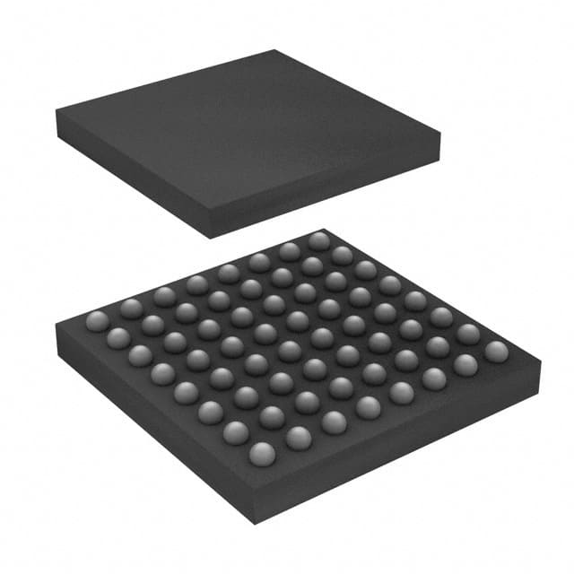
Pin Configuration (Detailed)
The S29GL01GP11FAIR12 flash memory chip has a total of 48 pins. The pin configuration is as follows:
- VCC: Power supply voltage
- A0-A18: Address inputs
- DQ0-DQ15: Data input/output lines
- WE#: Write enable control signal
- CE#: Chip enable control signal
- OE#: Output enable control signal
- RP#/BYTE#: Reset/byte enable control signal
- RY/BY#: Ready/busy status output
- WP#/ACC: Write protect/acceleration control
- VSS: Ground
(Note: This is a simplified representation. Please refer to the datasheet for the complete pin configuration.)
Functional Features
- High-speed read and write operations
- Sector erase capability for efficient data management
- Built-in error correction codes (ECC) for data integrity
- Low power consumption in standby mode
- Automatic program and erase algorithms for ease of use
Advantages and Disadvantages
Advantages: - Large storage capacity - Fast read/write speeds - Non-volatile memory retains data even without power - Reliable and durable - Suitable for a wide range of electronic devices
Disadvantages: - Limited erase/program cycles - Higher cost compared to other types of memory - Requires specific programming and erasing procedures
Working Principles
The S29GL01GP11FAIR12 flash memory utilizes floating-gate transistors to store data. It operates based on the principles of electrical charge trapping and tunneling. When data is written, charges are trapped in the floating gate, altering the transistor's conductive properties. During read operations, the stored charges are detected, allowing the retrieval of the stored data.
Detailed Application Field Plans
The S29GL01GP11FAIR12 flash memory chip finds applications in various electronic devices, including but not limited to: - Solid-state drives (SSDs) - Digital cameras - Mobile phones - Tablets - Gaming consoles - Automotive electronics - Industrial control systems
Alternative Models
- S29GL512P11TFI010: 512 Megabit (64 Megabytes) capacity, parallel interface
- S29GL02GP11FAIR20: 2 Gigabit (256 Megabytes) capacity, parallel interface
- S29GL04GP11FAIR40: 4 Gigabit (512 Megabytes) capacity, parallel interface
(Note: These are just a few examples. There are several alternative models available from different manufacturers.)
This concludes the encyclopedia entry for the S29GL01GP11FAIR12 flash memory chip.
Seznam 10 běžných otázek a odpovědí souvisejících s aplikací S29GL01GP11FAIR12 v technických řešeních
Sure! Here are 10 common questions and answers related to the application of S29GL01GP11FAIR12 in technical solutions:
Q: What is the S29GL01GP11FAIR12? A: The S29GL01GP11FAIR12 is a flash memory device manufactured by Cypress Semiconductor. It has a capacity of 1 gigabit and operates at a voltage range of 2.7V to 3.6V.
Q: What are the typical applications of S29GL01GP11FAIR12? A: The S29GL01GP11FAIR12 is commonly used in various technical solutions such as embedded systems, automotive electronics, industrial control systems, and consumer electronics.
Q: What is the interface of S29GL01GP11FAIR12? A: The S29GL01GP11FAIR12 uses a parallel interface with a multiplexed address and data bus. It supports both asynchronous and synchronous read and write operations.
Q: What is the operating temperature range of S29GL01GP11FAIR12? A: The S29GL01GP11FAIR12 can operate within a temperature range of -40°C to +85°C, making it suitable for a wide range of environments.
Q: Does S29GL01GP11FAIR12 support hardware and software data protection features? A: Yes, the S29GL01GP11FAIR12 provides hardware and software-based data protection mechanisms like block locking, password protection, and sector erase/program suspend/resume functions.
Q: What is the erase and program cycle endurance of S29GL01GP11FAIR12? A: The S29GL01GP11FAIR12 has a minimum endurance of 100,000 erase/program cycles per sector, ensuring reliable and long-lasting data storage.
Q: Can S29GL01GP11FAIR12 operate at different clock frequencies? A: Yes, the S29GL01GP11FAIR12 supports various clock frequencies, allowing flexibility in system design and integration.
Q: Does S29GL01GP11FAIR12 have any power-saving features? A: Yes, the S29GL01GP11FAIR12 offers several power-saving features like deep power-down mode, automatic sleep mode, and low-power standby mode to minimize power consumption.
Q: What is the package type of S29GL01GP11FAIR12? A: The S29GL01GP11FAIR12 is available in a 48-pin TSOP (Thin Small Outline Package) for easy integration into PCB designs.
Q: Is S29GL01GP11FAIR12 compatible with other flash memory devices? A: Yes, the S29GL01GP11FAIR12 is designed to be compatible with industry-standard flash memory devices, making it easy to replace or upgrade existing components in a system.
Please note that these answers are general and may vary depending on the specific implementation and requirements of your technical solution.