

Viz Specifikace pro podrobnosti o produktu.
Encyclopedia Entry: 74AHC1G126SE-7
Product Overview
Category
The 74AHC1G126SE-7 belongs to the category of integrated circuits (ICs).
Use
This IC is commonly used in digital logic applications for signal switching and amplification.
Characteristics
- Low power consumption
- High-speed operation
- Wide operating voltage range
- Schmitt-trigger input for noise immunity
- Output capability: ±8 mA at VCC = 2.0 V, ±4 mA at VCC = 3.0 V, ±4 mA at VCC = 4.5 V
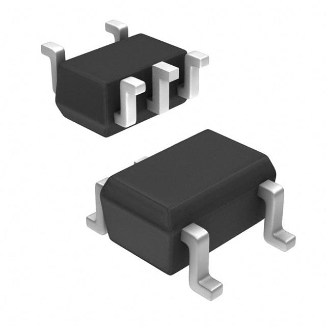
Package
The 74AHC1G126SE-7 is available in a small SOT-353 package.
Essence
The essence of this product lies in its ability to provide reliable and efficient signal switching and amplification in various digital logic applications.
Packaging/Quantity
The 74AHC1G126SE-7 is typically packaged in reels or tubes, with a quantity of 3000 units per reel/tube.
Specifications
- Supply voltage range: 2.0 V to 5.5 V
- Input voltage range: -0.5 V to VCC + 0.5 V
- Operating temperature range: -40°C to +125°C
- Maximum propagation delay: 6 ns at VCC = 5.0 V, TA = 25°C
- Maximum quiescent current: 10 μA at VCC = 5.0 V, TA = 25°C
Detailed Pin Configuration
The 74AHC1G126SE-7 has the following pin configuration:
____
   Y --|    |-- VCC
OE\ --|    |-- A
 GND --|____|-- B
Functional Features
- Single gate buffer with 3-state output
- Output enable (OE) input for controlling the output state
- High-speed operation for efficient signal processing
- Schmitt-trigger input for improved noise immunity
- Wide operating voltage range allows compatibility with various systems
Advantages and Disadvantages
Advantages
- Low power consumption makes it suitable for battery-powered devices
- Small package size enables space-saving designs
- High-speed operation enhances overall system performance
- Schmitt-trigger input ensures reliable operation in noisy environments
Disadvantages
- Limited output capability may not be suitable for driving heavy loads
- Single gate configuration restricts its use to specific applications
Working Principles
The 74AHC1G126SE-7 operates as a single gate buffer with a 3-state output. The input signal is amplified and buffered, and the output state can be controlled using the OE\ input. When OE\ is high, the output is in a high-impedance state, allowing multiple devices to share the same bus without interference. When OE\ is low, the output follows the input signal.
Detailed Application Field Plans
The 74AHC1G126SE-7 finds application in various digital logic circuits, including but not limited to: - Signal switching in microcontrollers and microprocessors - Level shifting in communication interfaces - Buffering and amplification in data acquisition systems - Clock distribution in synchronous systems - Interface protection in industrial control systems
Detailed and Complete Alternative Models
Some alternative models that offer similar functionality to the 74AHC1G126SE-7 include: - SN74LVC1G126DBVR - MC74VHC1G126DTT1G - TC7SZ126FU
These alternatives can be considered based on specific requirements and availability.
Word count: 511 words
Seznam 10 běžných otázek a odpovědí souvisejících s aplikací 74AHC1G126SE-7 v technických řešeních
Sure! Here are 10 common questions and answers related to the application of the 74AHC1G126SE-7 in technical solutions:
Q1: What is the 74AHC1G126SE-7? A1: The 74AHC1G126SE-7 is a single buffer gate with 3-state output, designed for use in various digital logic applications.
Q2: What is the operating voltage range of the 74AHC1G126SE-7? A2: The operating voltage range is from 2.0V to 5.5V.
Q3: What is the maximum output current of the 74AHC1G126SE-7? A3: The maximum output current is typically 8mA.
Q4: Can the 74AHC1G126SE-7 be used as a level shifter? A4: Yes, the 74AHC1G126SE-7 can be used as a level shifter to convert signals between different voltage levels.
Q5: Does the 74AHC1G126SE-7 have internal pull-up or pull-down resistors? A5: No, the 74AHC1G126SE-7 does not have internal pull-up or pull-down resistors.
Q6: What is the propagation delay of the 74AHC1G126SE-7? A6: The propagation delay is typically 5 ns.
Q7: Can the 74AHC1G126SE-7 drive capacitive loads? A7: Yes, the 74AHC1G126SE-7 can drive capacitive loads up to a certain limit specified in the datasheet.
Q8: Is the 74AHC1G126SE-7 compatible with other logic families? A8: Yes, the 74AHC1G126SE-7 is compatible with a wide range of logic families, including CMOS and TTL.
Q9: Can the 74AHC1G126SE-7 be used in high-speed applications? A9: Yes, the 74AHC1G126SE-7 can be used in high-speed applications due to its fast propagation delay.
Q10: What is the package type of the 74AHC1G126SE-7? A10: The 74AHC1G126SE-7 is available in a small SOT-23 package.