

Viz Specifikace pro podrobnosti o produktu.
Encyclopedia Entry: 74AUP1G04SE-7
Product Overview
Category
The 74AUP1G04SE-7 belongs to the category of integrated circuits (ICs) and specifically falls under the family of logic gates.
Use
This product is primarily used for signal amplification, inversion, and buffering in digital electronic circuits. It serves as a single inverter gate that can be employed in various applications.
Characteristics
- Low power consumption: The 74AUP1G04SE-7 operates at low voltage levels, resulting in reduced power consumption.
- High-speed operation: This IC offers fast switching times, making it suitable for high-frequency applications.
- Small form factor: The compact package size allows for space-efficient circuit designs.
- Wide operating voltage range: The device can operate within a broad voltage range, enhancing its versatility.
Package and Quantity
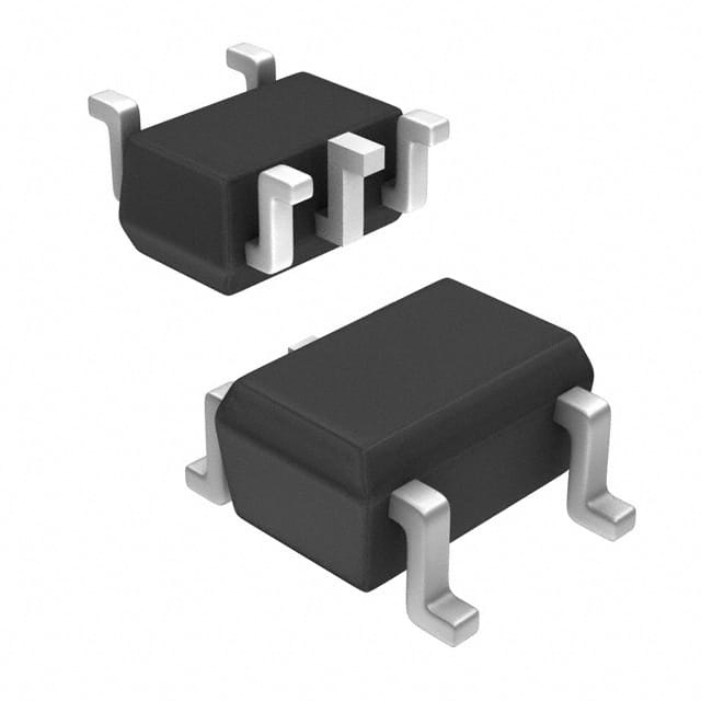
The 74AUP1G04SE-7 is available in a small surface-mount package, such as SOT-353 or SC-88A. It is typically sold in reels or tubes containing multiple units, with quantities varying based on the supplier.
Specifications
- Supply Voltage Range: 0.8V to 3.6V
- Input Voltage Range: 0V to VCC
- Output Voltage Range: 0V to VCC
- Maximum Operating Frequency: X MHz
- Input Capacitance: Y pF
- Output Current: Z mA
- Operating Temperature Range: -40°C to +85°C
Pin Configuration
The 74AUP1G04SE-7 features a standard pin configuration with the following pins:
- GND (Ground)
- IN (Input)
- OUT (Output)
- VCC (Power supply)
Functional Features
The primary function of the 74AUP1G04SE-7 is to invert the input signal received at the IN pin and provide the inverted output at the OUT pin. It operates as a digital buffer, ensuring compatibility between different logic families by converting voltage levels.
Advantages and Disadvantages
Advantages
- Low power consumption makes it suitable for battery-powered devices.
- High-speed operation enables efficient signal processing in time-critical applications.
- Small form factor allows for compact circuit designs.
- Wide operating voltage range enhances versatility.
Disadvantages
- Limited functionality: The 74AUP1G04SE-7 only serves as a single inverter gate and does not offer additional logic functions.
- Sensitivity to voltage fluctuations: The device may exhibit unpredictable behavior if operated outside the specified voltage range.
Working Principles
The 74AUP1G04SE-7 utilizes complementary metal-oxide-semiconductor (CMOS) technology to achieve its functionality. It consists of transistors that control the flow of current based on the input voltage level, resulting in the desired inversion of the signal.
Application Field Plans
The 74AUP1G04SE-7 finds application in various digital electronic circuits, including but not limited to: - Microcontrollers - Data communication systems - Signal amplification circuits - Clock generation circuits - Sensor interfaces
Alternative Models
For those seeking alternative options, several similar ICs can be considered: - 74LVC1G04: Offers similar functionality with slightly different specifications. - SN74LVC1G04: Another viable option with comparable characteristics. - NC7SZ04: A compact alternative with low power consumption.
These alternatives provide similar functionality and can be chosen based on specific project requirements.
In conclusion, the 74AUP1G04SE-7 is a versatile logic gate IC that offers low power consumption, high-speed operation, and a small form factor. Its primary function as an inverter gate makes it suitable for various digital electronic circuits. However, its limited functionality and sensitivity to voltage fluctuations should be considered. Alternative models such as 74LVC1G04, SN74LVC1G04, and NC7SZ04 can be explored based on specific project needs.
Seznam 10 běžných otázek a odpovědí souvisejících s aplikací 74AUP1G04SE-7 v technických řešeních
Sure! Here are 10 common questions and answers related to the application of 74AUP1G04SE-7 in technical solutions:
Q1: What is the 74AUP1G04SE-7? A1: The 74AUP1G04SE-7 is a single inverter gate IC (Integrated Circuit) that is commonly used in digital logic circuits.
Q2: What is the operating voltage range of the 74AUP1G04SE-7? A2: The operating voltage range of the 74AUP1G04SE-7 is typically between 0.8V and 3.6V.
Q3: What is the maximum output current of the 74AUP1G04SE-7? A3: The maximum output current of the 74AUP1G04SE-7 is around 32mA.
Q4: Can the 74AUP1G04SE-7 be used for level shifting? A4: Yes, the 74AUP1G04SE-7 can be used for level shifting as it supports both low-voltage and high-voltage operation.
Q5: Is the 74AUP1G04SE-7 suitable for battery-powered applications? A5: Yes, the 74AUP1G04SE-7 is suitable for battery-powered applications due to its low power consumption and wide operating voltage range.
Q6: What is the propagation delay of the 74AUP1G04SE-7? A6: The propagation delay of the 74AUP1G04SE-7 is typically around 2.5ns.
Q7: Can the 74AUP1G04SE-7 drive capacitive loads? A7: Yes, the 74AUP1G04SE-7 can drive capacitive loads up to a certain limit. However, it is recommended to use an external series resistor for better stability.
Q8: Is the 74AUP1G04SE-7 compatible with other logic families? A8: Yes, the 74AUP1G04SE-7 is compatible with various logic families such as CMOS, TTL, and LVCMOS.
Q9: Can the 74AUP1G04SE-7 be used in high-speed applications? A9: Yes, the 74AUP1G04SE-7 can be used in high-speed applications as it has a relatively fast switching speed.
Q10: What is the package type of the 74AUP1G04SE-7? A10: The 74AUP1G04SE-7 is available in a small SOT353 package, which is suitable for space-constrained designs.
Please note that these answers are general and may vary depending on specific application requirements.