

Viz Specifikace pro podrobnosti o produktu.
Encyclopedia Entry: 74AUP1G126FS3-7
Product Overview
Category
The 74AUP1G126FS3-7 belongs to the category of integrated circuits (ICs).
Use
This IC is commonly used for signal switching applications in various electronic devices.
Characteristics
- Low power consumption
- High-speed operation
- Wide operating voltage range
- Small package size
Package
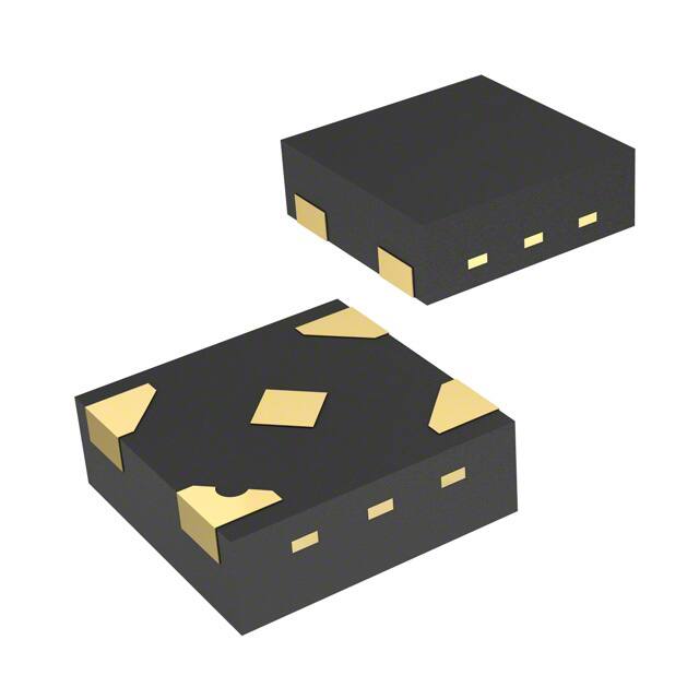
The 74AUP1G126FS3-7 is available in a small SOT-353 package.
Essence
This IC is designed to provide efficient and reliable signal switching capabilities in compact electronic systems.
Packaging/Quantity
The 74AUP1G126FS3-7 is typically packaged in reels, with each reel containing a specific quantity of ICs. The exact quantity may vary depending on the manufacturer's specifications.
Specifications
- Supply Voltage Range: 0.8V to 3.6V
- Input Voltage Range: -0.5V to VCC + 0.5V
- Output Voltage Range: -0.5V to VCC + 0.5V
- Maximum Operating Frequency: X MHz
- Operating Temperature Range: -40°C to +85°C
Detailed Pin Configuration
The 74AUP1G126FS3-7 has the following pin configuration:
```
| | --| A |-- --| Y |-- --| /OE |-- --| GND |-- --| VCC |-- |___________| ```
Pin Description: - A: Input pin for data signal - Y: Output pin for switched signal - /OE: Active-low enable pin for controlling the output state - GND: Ground connection - VCC: Power supply connection
Functional Features
- Single-channel signal switching
- High-speed operation for efficient data transmission
- Low power consumption for energy-efficient designs
- Wide operating voltage range allows compatibility with various systems
- Active-low enable pin for easy control of the output state
Advantages and Disadvantages
Advantages: - Low power consumption enhances battery life in portable devices. - High-speed operation enables fast data transfer. - Small package size saves valuable board space.
Disadvantages: - Limited number of input/output channels compared to multi-channel ICs. - May not be suitable for applications requiring complex signal routing.
Working Principles
The 74AUP1G126FS3-7 operates based on CMOS (Complementary Metal-Oxide-Semiconductor) technology. It utilizes MOSFET transistors to control the flow of signals, allowing for efficient switching between input and output states.
Detailed Application Field Plans
The 74AUP1G126FS3-7 finds applications in various electronic systems, including but not limited to: 1. Mobile phones and smartphones 2. Tablets and laptops 3. Digital cameras 4. Portable gaming consoles 5. Wearable devices
Detailed and Complete Alternative Models
- 74AUP1G126GW
- SN74AUP1G126DCKR
- MC74AUP1G126GM
- TC74AUP1G126FK
These alternative models offer similar functionality and can be used as substitutes for the 74AUP1G126FS3-7 in different applications.
In conclusion, the 74AUP1G126FS3-7 is a versatile integrated circuit that provides efficient signal switching capabilities in compact electronic systems. Its low power consumption, high-speed operation, and wide operating voltage range make it suitable for a variety of applications. However, its limited number of channels and potential unsuitability for complex signal routing should be considered when selecting this IC for specific projects.
Seznam 10 běžných otázek a odpovědí souvisejících s aplikací 74AUP1G126FS3-7 v technických řešeních
Sure! Here are 10 common questions and answers related to the application of 74AUP1G126FS3-7 in technical solutions:
Q1: What is the 74AUP1G126FS3-7? A1: The 74AUP1G126FS3-7 is a single bus buffer gate with three-state output, designed for low-power applications.
Q2: What is the operating voltage range of the 74AUP1G126FS3-7? A2: The operating voltage range is from 0.8V to 3.6V.
Q3: What is the maximum output current of the 74AUP1G126FS3-7? A3: The maximum output current is 32mA.
Q4: Can the 74AUP1G126FS3-7 be used as a level shifter? A4: Yes, the 74AUP1G126FS3-7 can be used as a level shifter between different voltage domains.
Q5: What is the propagation delay of the 74AUP1G126FS3-7? A5: The typical propagation delay is 2.9ns.
Q6: Can the 74AUP1G126FS3-7 be used in high-speed applications? A6: No, the 74AUP1G126FS3-7 is not recommended for high-speed applications due to its relatively slow propagation delay.
Q7: Does the 74AUP1G126FS3-7 have an internal pull-up or pull-down resistor? A7: No, the 74AUP1G126FS3-7 does not have an internal pull-up or pull-down resistor.
Q8: Can the 74AUP1G126FS3-7 be used in bidirectional applications? A8: No, the 74AUP1G126FS3-7 is a unidirectional buffer and cannot be used for bidirectional communication.
Q9: What is the package type of the 74AUP1G126FS3-7? A9: The 74AUP1G126FS3-7 is available in a small SOT353 package.
Q10: Can the 74AUP1G126FS3-7 drive capacitive loads? A10: Yes, the 74AUP1G126FS3-7 can drive capacitive loads up to 50pF.
Please note that these answers are based on general information about the 74AUP1G126FS3-7. It's always recommended to refer to the datasheet or consult the manufacturer for specific details and application guidelines.