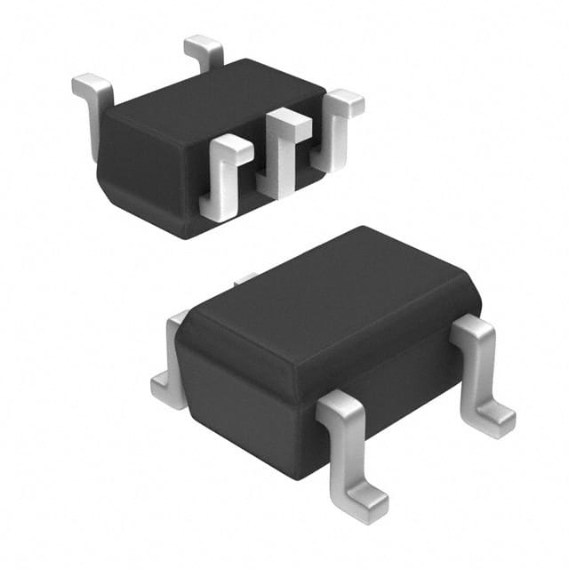
Viz Specifikace pro podrobnosti o produktu.

Encyclopedia Entry: 74AUP1G17SE-7
Product Overview
Category
The 74AUP1G17SE-7 belongs to the category of integrated circuits (ICs) and specifically falls under the family of logic gates.
Use
This product is commonly used in digital electronics for signal processing and logical operations. It serves as a buffer or driver, ensuring proper voltage levels and signal integrity between different components of a circuit.
Characteristics
- Single gate logic buffer/driver
- Low power consumption
- High-speed operation
- Wide operating voltage range
- Small package size
- RoHS compliant
Package and Quantity
The 74AUP1G17SE-7 is available in a small surface-mount package, such as SOT353 or SC-88A. It is typically sold in reels or tubes containing multiple units, with quantities varying based on manufacturer and distributor specifications.
Essence
The essence of the 74AUP1G17SE-7 lies in its ability to provide reliable signal buffering and driving capabilities in various digital electronic applications. Its compact size, low power consumption, and high-speed operation make it an ideal choice for space-constrained and power-sensitive designs.
Specifications
- Supply Voltage Range: 0.8V to 3.6V
- Input Voltage Range: 0V to VCC
- Output Voltage Range: 0V to VCC
- Maximum Operating Frequency: X MHz
- Propagation Delay: Y ns
- Operating Temperature Range: -40°C to +85°C
- Input/Output Logic Levels: CMOS/TTL compatible
Detailed Pin Configuration
The 74AUP1G17SE-7 consists of a single gate with the following pin configuration:
____
   A --|    |-- VCC
   Y --|    |-- GND
       ----
Functional Features
- Buffering: The 74AUP1G17SE-7 acts as a buffer, ensuring that the input signal is not affected by the load connected to its output.
- Driving: It provides sufficient current to drive capacitive loads and maintain signal integrity across the circuit.
- Logic Level Shifting: The IC can convert logic levels between different voltage domains, allowing compatibility between devices operating at different voltage levels.
Advantages and Disadvantages
Advantages
- Low power consumption makes it suitable for battery-powered devices.
- High-speed operation enables efficient data processing.
- Wide operating voltage range allows compatibility with various systems.
- Small package size saves board space in compact designs.
- RoHS compliance ensures environmental friendliness.
Disadvantages
- Limited number of gates per package compared to larger ICs.
- May require additional components for certain applications, such as pull-up or pull-down resistors.
Working Principles
The 74AUP1G17SE-7 operates based on CMOS (Complementary Metal-Oxide-Semiconductor) technology. It utilizes MOSFET transistors to control the flow of current, enabling the buffering and driving functions. The input signal is amplified and then transmitted to the output with minimal distortion.
Detailed Application Field Plans
The 74AUP1G17SE-7 finds application in various digital electronic systems, including but not limited to: - Mobile devices - Wearable electronics - Internet of Things (IoT) devices - Automotive electronics - Industrial automation - Consumer electronics
Detailed Alternative Models
Several alternative models are available in the market that offer similar functionality to the 74AUP1G17SE-7. Some notable alternatives include: - 74LVC1G17GW - SN74LVC1G17DBVR - MC74VHC1G17DTT1G
These alternatives may differ in terms of package type, voltage range, speed, and other specifications. It is important to select the most suitable alternative based on specific application requirements.
Word Count: 536 words
Seznam 10 běžných otázek a odpovědí souvisejících s aplikací 74AUP1G17SE-7 v technických řešeních
Sure! Here are 10 common questions and answers related to the application of 74AUP1G17SE-7 in technical solutions:
Q1: What is the 74AUP1G17SE-7? A1: The 74AUP1G17SE-7 is a single Schmitt-trigger buffer with open-drain output, designed for low-power applications.
Q2: What is the operating voltage range of the 74AUP1G17SE-7? A2: The operating voltage range is from 0.8V to 3.6V.
Q3: What is the maximum output current of the 74AUP1G17SE-7? A3: The maximum output current is typically 32mA.
Q4: Can the 74AUP1G17SE-7 be used as a level shifter? A4: Yes, the 74AUP1G17SE-7 can be used as a level shifter between different voltage domains.
Q5: What is the propagation delay of the 74AUP1G17SE-7? A5: The propagation delay is typically 2.5ns.
Q6: Is the 74AUP1G17SE-7 suitable for high-speed applications? A6: No, the 74AUP1G17SE-7 is not recommended for high-speed applications due to its relatively slow propagation delay.
Q7: Can the 74AUP1G17SE-7 be used in battery-powered devices? A7: Yes, the 74AUP1G17SE-7 is designed for low-power applications and can be used in battery-powered devices.
Q8: Does the 74AUP1G17SE-7 have built-in ESD protection? A8: Yes, the 74AUP1G17SE-7 has built-in ESD protection up to 2kV.
Q9: Can the 74AUP1G17SE-7 drive capacitive loads? A9: Yes, the 74AUP1G17SE-7 can drive capacitive loads up to 50pF.
Q10: What is the package type of the 74AUP1G17SE-7? A10: The 74AUP1G17SE-7 is available in a small SOT353 package.
Please note that these answers are general and may vary depending on the specific datasheet and manufacturer's specifications.

