

Viz Specifikace pro podrobnosti o produktu.
Encyclopedia Entry: 74AUP1G86FW5-7
Product Overview
- Category: Integrated Circuit (IC)
- Use: Logic Gate
- Characteristics: Single 2-input XOR gate
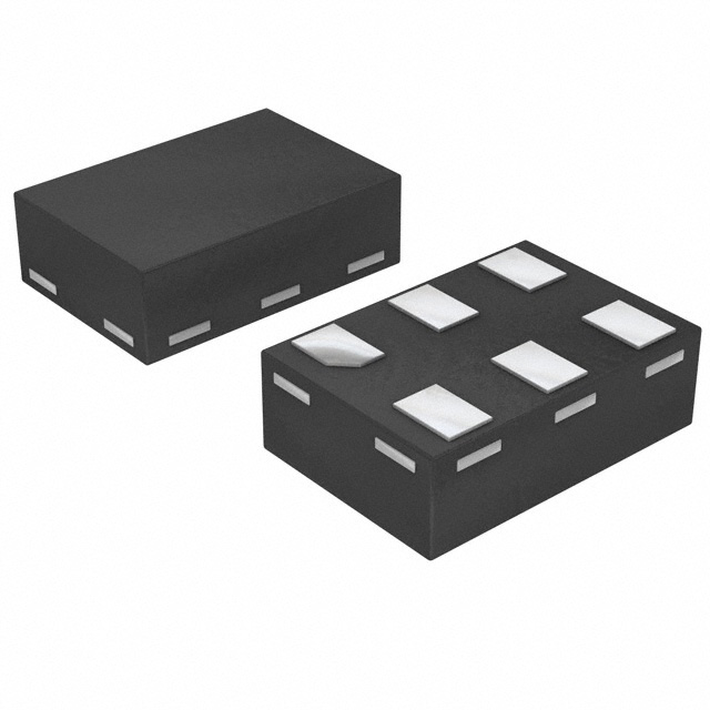
- Package: SOT353 (SC-88A)
- Essence: High-speed CMOS technology
- Packaging/Quantity: Tape and Reel, 3000 pieces per reel
Specifications
- Supply Voltage Range: 0.8V to 3.6V
- Input Voltage Range: -0.5V to VCC + 0.5V
- Output Voltage Range: 0V to VCC
- Operating Temperature Range: -40°C to +125°C
- Propagation Delay: 4.5 ns (typical) at VCC = 3.3V, TA = 25°C
- Quiescent Current: 10 µA (typical) at VCC = 3.3V, TA = 25°C
Detailed Pin Configuration
The 74AUP1G86FW5-7 has a total of 5 pins: 1. Pin 1: Input A 2. Pin 2: Input B 3. Pin 3: Ground (GND) 4. Pin 4: Output Y 5. Pin 5: Power Supply (VCC)
Functional Features
- Performs exclusive OR (XOR) operation on two input signals (A and B)
- Provides a single output signal (Y) based on the XOR operation result
- High-speed operation due to the utilization of advanced CMOS technology
- Low power consumption with a quiescent current of only 10 µA
Advantages and Disadvantages
Advantages: - Compact size and lightweight package (SOT353) - Wide supply voltage range allows for versatile applications - High-speed operation enables efficient signal processing - Low power consumption contributes to energy efficiency
Disadvantages: - Limited number of inputs (only 2) - Not suitable for complex logic operations requiring multiple gates
Working Principles
The 74AUP1G86FW5-7 is based on high-speed CMOS technology, which utilizes complementary metal-oxide-semiconductor transistors to perform logical operations. In the case of this specific IC, it functions as a XOR gate. The XOR gate compares two input signals and produces an output signal that is high (logic level 1) only when the inputs differ. The IC operates within a specified supply voltage range and provides fast propagation delay and low power consumption.
Detailed Application Field Plans
The 74AUP1G86FW5-7 can be used in various applications where XOR logic operations are required. Some potential application fields include: 1. Digital communication systems 2. Data encryption and decryption circuits 3. Error detection and correction circuits 4. Arithmetic and mathematical operations 5. Control and automation systems
Detailed and Complete Alternative Models
- 74AUP1G86GM
- 74AUP1G86GW
- 74AUP1G86GF
- 74AUP1G86GN
- 74AUP1G86GX
These alternative models offer similar functionality and characteristics to the 74AUP1G86FW5-7, providing options for different package types or minor variations in specifications.
Word count: 346 words
Seznam 10 běžných otázek a odpovědí souvisejících s aplikací 74AUP1G86FW5-7 v technických řešeních
Sure! Here are 10 common questions and answers related to the application of 74AUP1G86FW5-7 in technical solutions:
Q1: What is the 74AUP1G86FW5-7? A1: The 74AUP1G86FW5-7 is a single 2-input XOR gate IC (integrated circuit) that operates at a voltage range of 0.8V to 3.6V.
Q2: What is the purpose of the 74AUP1G86FW5-7? A2: The purpose of this IC is to perform XOR (exclusive OR) logic operations, which are commonly used in digital circuits for various applications such as data encryption, error detection, and signal processing.
Q3: What is the maximum operating frequency of the 74AUP1G86FW5-7? A3: The maximum operating frequency of this IC is typically around 500 MHz, making it suitable for high-speed digital applications.
Q4: Can the 74AUP1G86FW5-7 be used with different supply voltages? A4: Yes, the 74AUP1G86FW5-7 can operate with a wide range of supply voltages, from 0.8V to 3.6V, allowing flexibility in various system designs.
Q5: How many inputs does the 74AUP1G86FW5-7 have? A5: The 74AUP1G86FW5-7 has two inputs, labeled A and B, which are used for the XOR operation.
Q6: What is the output voltage level of the 74AUP1G86FW5-7? A6: The output voltage level of this IC is compatible with both CMOS (Complementary Metal-Oxide-Semiconductor) and TTL (Transistor-Transistor Logic) logic levels.
Q7: Can the 74AUP1G86FW5-7 be used in battery-powered applications? A7: Yes, the 74AUP1G86FW5-7 is designed to operate at low power consumption, making it suitable for battery-powered applications where energy efficiency is crucial.
Q8: Is the 74AUP1G86FW5-7 available in different package types? A8: Yes, this IC is available in various package types, such as SOT353, XSON6, and DFN6, providing options for different PCB (Printed Circuit Board) layouts and space constraints.
Q9: What is the propagation delay of the 74AUP1G86FW5-7? A9: The typical propagation delay of this IC is around 2.5 ns, which indicates the time taken for the output to respond to a change in the input signals.
Q10: Can the 74AUP1G86FW5-7 be cascaded with other logic gates? A10: Yes, the 74AUP1G86FW5-7 can be cascaded with other logic gates to create more complex digital circuits, allowing for versatile system designs.
Please note that the answers provided here are general and may vary depending on specific datasheet specifications or application requirements.