

Viz Specifikace pro podrobnosti o produktu.
74LVC1G00FZ4-7
Product Overview
Category
The 74LVC1G00FZ4-7 belongs to the category of integrated circuits (ICs).
Use
This IC is commonly used in digital logic applications.
Characteristics
- Low voltage CMOS technology
- High-speed operation
- Wide operating voltage range
- Low power consumption
- Schmitt-trigger input for noise immunity
- Small package size
Package
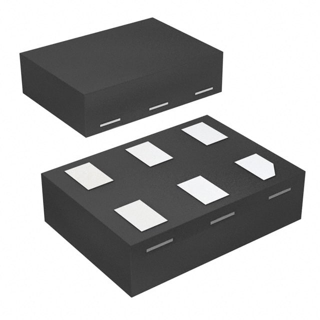
The 74LVC1G00FZ4-7 is available in a small form factor SOT-353 package.
Essence
The essence of the 74LVC1G00FZ4-7 lies in its ability to perform logical AND operations on two input signals.
Packaging/Quantity
This IC is typically packaged in reels or tubes, with a quantity of 3000 units per reel/tube.
Specifications
- Supply Voltage: 1.65V to 5.5V
- Input Voltage: 0V to VCC
- Output Voltage: 0V to VCC
- Operating Temperature Range: -40°C to +125°C
- Propagation Delay: 3.8ns (typical)
- Maximum Quiescent Current: 10μA
Detailed Pin Configuration
The 74LVC1G00FZ4-7 has a total of 5 pins:
- GND (Ground)
- A (Input A)
- B (Input B)
- Y (Output)
- VCC (Supply Voltage)
Functional Features
The main functional feature of the 74LVC1G00FZ4-7 is its ability to perform logical AND operations. It takes two input signals, A and B, and produces an output signal, Y, which represents the logical AND of A and B.
Advantages
- Low power consumption makes it suitable for battery-powered devices.
- Wide operating voltage range allows compatibility with various systems.
- Schmitt-trigger input provides noise immunity, ensuring reliable operation in noisy environments.
- Small package size saves board space in compact designs.
Disadvantages
- Limited number of inputs (only two) restricts its application in complex logic circuits.
- Propagation delay may affect timing-sensitive applications.
Working Principles
The 74LVC1G00FZ4-7 utilizes CMOS technology to implement the logical AND function. When both input signals, A and B, are high, the output signal, Y, is also high. Otherwise, the output remains low.
Detailed Application Field Plans
The 74LVC1G00FZ4-7 finds applications in various digital logic circuits, including but not limited to: - Multiplexers - Encoders - Decoders - Flip-flops - Counters - Data selectors
Detailed and Complete Alternative Models
Some alternative models that can be used as substitutes for the 74LVC1G00FZ4-7 include: - SN74LVC1G00DBVR - MC74VHC1G00DTT1G - TC7SZ00FU
These alternatives offer similar functionality and characteristics, providing flexibility in design choices.
In conclusion, the 74LVC1G00FZ4-7 is a versatile integrated circuit that performs logical AND operations. Its low power consumption, wide operating voltage range, and small package size make it suitable for various digital logic applications. However, its limited number of inputs and propagation delay should be considered when selecting this IC for specific designs.
Seznam 10 běžných otázek a odpovědí souvisejících s aplikací 74LVC1G00FZ4-7 v technických řešeních
Sure! Here are 10 common questions and answers related to the application of 74LVC1G00FZ4-7 in technical solutions:
Q1: What is the 74LVC1G00FZ4-7? A1: The 74LVC1G00FZ4-7 is a single 2-input NAND gate IC (integrated circuit) that operates at 3.3V voltage levels.
Q2: What is the maximum operating frequency of the 74LVC1G00FZ4-7? A2: The maximum operating frequency of the 74LVC1G00FZ4-7 is typically around 400 MHz.
Q3: Can the 74LVC1G00FZ4-7 be used with both CMOS and TTL logic levels? A3: Yes, the 74LVC1G00FZ4-7 is compatible with both CMOS and TTL logic levels, making it versatile for various applications.
Q4: What is the power supply voltage range for the 74LVC1G00FZ4-7? A4: The power supply voltage range for the 74LVC1G00FZ4-7 is from 1.65V to 5.5V.
Q5: How many inputs does the 74LVC1G00FZ4-7 have? A5: The 74LVC1G00FZ4-7 has two inputs, making it a 2-input NAND gate.
Q6: What is the output drive capability of the 74LVC1G00FZ4-7? A6: The 74LVC1G00FZ4-7 has a typical output drive capability of ±24mA.
Q7: Can the 74LVC1G00FZ4-7 be used in high-speed applications? A7: Yes, the 74LVC1G00FZ4-7 is designed for high-speed operation and can be used in various high-speed applications.
Q8: Is the 74LVC1G00FZ4-7 available in different package options? A8: Yes, the 74LVC1G00FZ4-7 is available in different package options, such as SOT353 and XSON6.
Q9: What is the typical propagation delay of the 74LVC1G00FZ4-7? A9: The typical propagation delay of the 74LVC1G00FZ4-7 is around 3.5 ns.
Q10: Can the 74LVC1G00FZ4-7 be used in battery-powered applications? A10: Yes, the 74LVC1G00FZ4-7 operates at low power consumption and can be used in battery-powered applications.
Please note that the answers provided here are general and may vary depending on specific datasheet specifications and application requirements.