

Viz Specifikace pro podrobnosti o produktu.
Encyclopedia Entry: 74LVC1G08FZ4-7
Product Overview
The 74LVC1G08FZ4-7 is an integrated circuit (IC) belonging to the category of logic gates. It is specifically designed for use in digital electronics applications. This IC serves as a single 2-input AND gate, making it an essential component in various electronic circuits.
Characteristics
- Category: Logic Gates
- Use: Digital Electronics
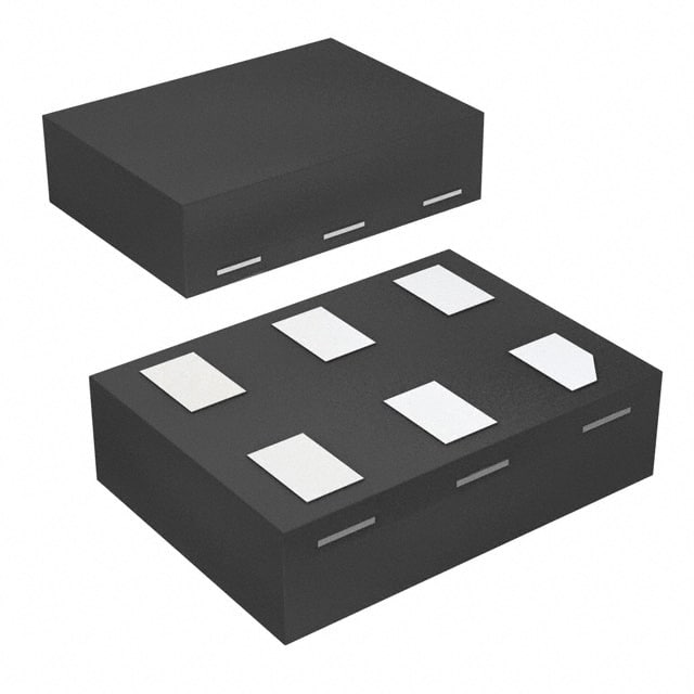
- Package: SOT-353
- Essence: Single 2-input AND Gate
- Packaging/Quantity: Tape and Reel, 3000 pieces per reel
Specifications
- Supply Voltage Range: 1.65V to 5.5V
- High-Level Input Voltage: 0.7 x VCC
- Low-Level Input Voltage: 0.3 x VCC
- High-Level Output Current: -32mA
- Low-Level Output Current: 32mA
- Propagation Delay: 4.3ns (typical)
Detailed Pin Configuration
The 74LVC1G08FZ4-7 IC has a total of 5 pins, each serving a specific function: 1. Pin 1: Input A 2. Pin 2: Input B 3. Pin 3: Ground (GND) 4. Pin 4: Output Y 5. Pin 5: Power Supply (VCC)
Functional Features
- Single 2-input AND gate functionality
- Wide supply voltage range allows compatibility with various systems
- High-speed operation with low propagation delay
- Balanced output drive capability for improved noise immunity
- Schmitt-trigger input for hysteresis and increased noise tolerance
Advantages and Disadvantages
Advantages: - Compact size and low power consumption - Versatile application possibilities - Excellent noise immunity due to Schmitt-trigger input
Disadvantages: - Limited number of inputs (2-input only) - Not suitable for complex logic operations requiring multiple gates
Working Principles
The 74LVC1G08FZ4-7 operates based on the principles of Boolean logic. It performs the logical AND operation on its two input signals, A and B, and produces a corresponding output signal, Y. The IC utilizes transistors and other electronic components to achieve this functionality.
Detailed Application Field Plans
The 74LVC1G08FZ4-7 finds extensive use in various digital electronics applications, including but not limited to: - Microcontrollers and microprocessors - Data communication systems - Industrial automation - Consumer electronics - Automotive electronics
Detailed Alternative Models
For those seeking alternative options, several similar ICs can be considered as replacements or alternatives to the 74LVC1G08FZ4-7. Some notable alternatives include: - SN74LVC1G08DBVR - MC74VHC1G08DTT1G - TC7SZ08FU
These alternatives offer similar functionality and characteristics, providing flexibility in design choices.
In conclusion, the 74LVC1G08FZ4-7 is a compact and versatile logic gate IC widely used in digital electronics applications. Its single 2-input AND gate functionality, along with its excellent noise immunity and low power consumption, make it an essential component in various electronic circuits.
Seznam 10 běžných otázek a odpovědí souvisejících s aplikací 74LVC1G08FZ4-7 v technických řešeních
Sure! Here are 10 common questions and answers related to the application of the 74LVC1G08FZ4-7 in technical solutions:
Q1: What is the 74LVC1G08FZ4-7? A1: The 74LVC1G08FZ4-7 is a single 2-input AND gate IC (integrated circuit) that operates at 3.3V or 5V supply voltage.
Q2: What is the purpose of an AND gate? A2: An AND gate is a logic gate that produces a high output only when all its inputs are high.
Q3: What are the typical applications of the 74LVC1G08FZ4-7? A3: The 74LVC1G08FZ4-7 can be used in various applications such as signal conditioning, level shifting, data routing, and general-purpose logic functions.
Q4: What is the maximum operating frequency of the 74LVC1G08FZ4-7? A4: The maximum operating frequency of the 74LVC1G08FZ4-7 is typically around 500 MHz.
Q5: What is the input voltage range for the 74LVC1G08FZ4-7? A5: The input voltage range for the 74LVC1G08FZ4-7 is from ground (0V) to the supply voltage (3.3V or 5V).
Q6: Can the 74LVC1G08FZ4-7 handle multiple power supplies? A6: No, the 74LVC1G08FZ4-7 is designed to operate with a single power supply.
Q7: What is the output drive capability of the 74LVC1G08FZ4-7? A7: The 74LVC1G08FZ4-7 has a typical output drive capability of 32 mA.
Q8: Can the 74LVC1G08FZ4-7 be used in both CMOS and TTL logic systems? A8: Yes, the 74LVC1G08FZ4-7 is compatible with both CMOS and TTL logic levels.
Q9: Is the 74LVC1G08FZ4-7 available in different package options? A9: Yes, the 74LVC1G08FZ4-7 is available in various package options such as SOT353, SC-88A, and XSON6.
Q10: What are the temperature range and storage conditions for the 74LVC1G08FZ4-7? A10: The operating temperature range for the 74LVC1G08FZ4-7 is typically -40°C to +125°C, and it should be stored in a dry environment at temperatures between -55°C and +150°C.
Please note that the answers provided here are general and may vary depending on the specific datasheet and manufacturer's specifications for the 74LVC1G08FZ4-7.