

Viz Specifikace pro podrobnosti o produktu.
74LVC2G04DW-7
Product Overview
Category
The 74LVC2G04DW-7 belongs to the category of integrated circuits (ICs) and specifically falls under the logic gates family.
Use
This product is commonly used in digital electronic circuits for signal inversion and buffering purposes. It is primarily employed to convert input signals into their complementary form.
Characteristics
- Low-voltage CMOS technology
- High-speed operation
- Wide operating voltage range
- Low power consumption
- Schmitt-trigger action on inputs
- Balanced propagation delays
- Symmetrical output impedance
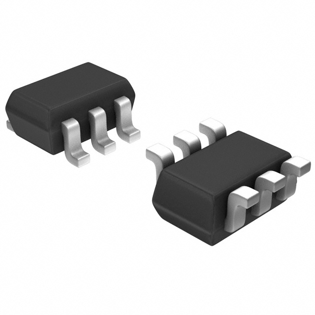
Package
The 74LVC2G04DW-7 is available in a small-sized package known as "TSSOP" (Thin Shrink Small Outline Package). This package offers excellent thermal performance and allows for easy integration into various circuit designs.
Essence
The essence of this product lies in its ability to provide reliable and efficient signal inversion and buffering functions, making it an essential component in digital electronic systems.
Packaging/Quantity
The 74LVC2G04DW-7 is typically supplied in reels or tubes, with each reel containing a specific quantity of ICs. The exact quantity may vary depending on the manufacturer and customer requirements.
Specifications
- Supply Voltage Range: 1.65V to 5.5V
- Input Voltage Range: 0V to VCC
- Output Voltage Range: 0V to VCC
- Operating Temperature Range: -40°C to +125°C
- Maximum Propagation Delay: 4.3 ns (at 5V)
- Maximum Quiescent Current: 10 μA (at 5V)
Detailed Pin Configuration
The 74LVC2G04DW-7 has a total of 6 pins, which are labeled as follows:
- GND (Ground)
- A (Input A)
- Y (Output Y)
- VCC (Supply Voltage)
- B (Input B)
- GND (Ground)
Functional Features
- Signal inversion: The 74LVC2G04DW-7 can invert the logic level of input signals, providing their complementary form at the output.
- Buffering: It acts as a buffer, isolating the input from the output and enhancing signal integrity.
Advantages and Disadvantages
Advantages
- Low power consumption makes it suitable for battery-powered devices.
- Wide operating voltage range allows compatibility with various systems.
- Schmitt-trigger action on inputs ensures noise immunity.
- Balanced propagation delays enable precise timing in digital circuits.
Disadvantages
- Limited number of inputs and outputs restricts its application in complex systems.
- Not suitable for high-voltage applications due to its low-voltage CMOS technology.
Working Principles
The 74LVC2G04DW-7 operates based on complementary metal-oxide-semiconductor (CMOS) technology. It utilizes a combination of transistors to achieve signal inversion and buffering. When an input signal is applied, the internal circuitry processes it and generates the complementary output signal.
Detailed Application Field Plans
The 74LVC2G04DW-7 finds extensive use in various digital electronic applications, including but not limited to: - Microcontrollers - Data communication systems - Industrial automation - Consumer electronics - Automotive electronics
Detailed and Complete Alternative Models
Some alternative models that offer similar functionality to the 74LVC2G04DW-7 include: - SN74LVC2G04DBVR - MC74VHC1G04DFT1G - TC7SZ04FU
These alternatives can be considered based on specific requirements and availability.
Word count: 422
Seznam 10 běžných otázek a odpovědí souvisejících s aplikací 74LVC2G04DW-7 v technických řešeních
Sure! Here are 10 common questions and answers related to the application of 74LVC2G04DW-7 in technical solutions:
Q: What is the 74LVC2G04DW-7? A: The 74LVC2G04DW-7 is a dual inverter gate IC, which can be used for signal inversion or buffering in digital circuits.
Q: What is the operating voltage range of the 74LVC2G04DW-7? A: The operating voltage range is typically between 1.65V and 5.5V.
Q: What is the maximum output current of the 74LVC2G04DW-7? A: The maximum output current is around 32mA.
Q: Can the 74LVC2G04DW-7 be used in high-speed applications? A: Yes, the 74LVC2G04DW-7 is designed for high-speed operation and has a propagation delay of only a few nanoseconds.
Q: How many inverters are there in the 74LVC2G04DW-7? A: The 74LVC2G04DW-7 contains two independent inverters.
Q: Can the 74LVC2G04DW-7 be used in battery-powered devices? A: Yes, the 74LVC2G04DW-7 has a low power consumption and can be used in battery-powered applications.
Q: What is the package type of the 74LVC2G04DW-7? A: The 74LVC2G04DW-7 is available in a small SOT-363 package.
Q: Is the 74LVC2G04DW-7 compatible with other logic families? A: Yes, the 74LVC2G04DW-7 is compatible with both CMOS and TTL logic families.
Q: Can the 74LVC2G04DW-7 be used in automotive applications? A: Yes, the 74LVC2G04DW-7 is qualified for automotive applications and can operate in a wide temperature range.
Q: What are some typical applications of the 74LVC2G04DW-7? A: The 74LVC2G04DW-7 can be used in various applications such as signal inversion, level shifting, clock buffering, and general-purpose digital logic circuits.
Please note that these answers are general and may vary depending on specific datasheet specifications and application requirements.