

Viz Specifikace pro podrobnosti o produktu.
PI6C49S1506FAIE
Overview
- Category: Integrated Circuit
- Use: Clock Generator and Buffer
- Characteristics: Low jitter, high frequency accuracy, low power consumption
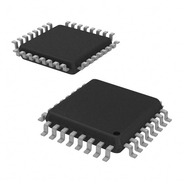
- Package: QFN (Quad Flat No-leads)
- Essence: Clock generation and buffering for electronic devices
- Packaging/Quantity: Tape and Reel, 2500 pieces per reel
Specifications and Parameters
- Frequency Range: 1 MHz to 200 MHz
- Supply Voltage: 1.8 V to 3.3 V
- Output Type: LVCMOS
- Operating Temperature Range: -40°C to +85°C
Pin Configuration
The PI6C49S1506FAIE has a total of 32 pins. The pin configuration is as follows:
- VDD
- GND
- OUT0
- OUT1
- OUT2
- OUT3
- OUT4
- OUT5
- OUT6
- OUT7
- OUT8
- OUT9
- OUT10
- OUT11
- OUT12
- OUT13
- OUT14
- OUT15
- OE
- SDA
- SCL
- VDD
- GND
- NC
- NC
- NC
- NC
- NC
- NC
- NC
- NC
- NC
Functional Characteristics
- Generates up to 16 clock outputs with programmable frequencies
- Supports I2C interface for easy configuration
- Low jitter and high frequency accuracy for precise timing requirements
- Low power consumption for energy-efficient designs
Advantages and Disadvantages
Advantages: - Flexible clock generation with multiple output options - Easy configuration through I2C interface - High accuracy and low jitter for precise timing applications
Disadvantages: - Limited frequency range compared to some other clock generators - Requires external components for proper operation
Applicable Range of Products
The PI6C49S1506FAIE is suitable for a wide range of electronic devices that require accurate clock generation and buffering. It can be used in various applications such as communication systems, computer peripherals, consumer electronics, and industrial equipment.
Working Principles
The PI6C49S1506FAIE utilizes an internal oscillator and phase-locked loop (PLL) to generate stable clock signals. The PLL locks onto an input reference clock and generates multiple output clocks with programmable frequencies. The I2C interface allows users to configure the desired output frequencies and other parameters.
Detailed Application Field Plans
- Communication Systems: Use the PI6C49S1506FAIE to generate clock signals for data transmission and reception in wireless communication systems.
- Computer Peripherals: Utilize the device to provide accurate timing signals for USB interfaces, Ethernet ports, and other peripheral devices.
- Consumer Electronics: Incorporate the chip into audio/video equipment, gaming consoles, and smart home devices to ensure precise synchronization and timing.
- Industrial Equipment: Employ the PI6C49S1506FAIE in industrial automation systems, test and measurement instruments, and control systems for reliable timing and synchronization.
- Automotive Electronics: Use the chip in automotive applications such as infotainment systems, advanced driver-assistance systems (ADAS), and engine control units (ECUs) to maintain accurate timing.
Detailed Alternative Models
- PI6C49S1506FAGIE: Similar to PI6C49S1506FAIE but with extended temperature range (-40°C to +105°C).
- PI6C49S1506FBIE: Lower power version of PI6C49S1506FAIE with reduced supply voltage range (1.2 V to 3.3 V).
- PI6C49S1506FCIE: Higher frequency version of PI6C49S1506FAIE with extended frequency range (1 MHz to 500 MHz).
5 Common Technical Questions and Answers
Q: What is the maximum number of clock outputs supported by the PI6C49S1506FAIE? A: The chip can generate up to 16 clock outputs.
Q: Can I program the output frequencies dynamically during operation? A: Yes, the device supports dynamic frequency programming through the I2C interface.
Q: Is an external crystal oscillator required for the PI6C49S1506FAIE? A: No, the chip has an internal oscillator that can be used as a reference clock.
Q: What is the typical jitter performance of the PI6C49S1506FAIE? A: The chip offers low jitter performance, typically below 100 ps.
Q: