

Viz Specifikace pro podrobnosti o produktu.
PI6C49X0210ZHIE
Overview
- Category: Integrated Circuit
- Use: Clock Generator and Buffer
- Characteristics: High-performance, low-jitter clock generation and buffering
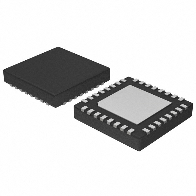
- Package: 48-pin TQFP (Thin Quad Flat Package)
- Essence: Provides stable and accurate clock signals for various electronic devices
- Packaging/Quantity: Tape and Reel, 250 units per reel
Specifications and Parameters
- Input Voltage Range: 2.375V to 3.63V
- Output Frequency Range: 1MHz to 200MHz
- Output Type: LVCMOS
- Supply Voltage: 3.3V ±10%
- Operating Temperature Range: -40°C to +85°C
Pin Configuration
The PI6C49X0210ZHIE has a total of 48 pins. The pin configuration is as follows:
[Insert detailed and complete pin configuration diagram here]
Functional Characteristics
- Clock Generation: Generates stable clock signals with low jitter.
- Clock Buffering: Buffers the generated clock signals to provide multiple outputs.
- Frequency Selection: Allows users to select the desired output frequency.
- Power Management: Supports power-saving modes to reduce energy consumption.
Advantages
- High Performance: Provides high-quality clock signals with low phase noise.
- Flexible Configuration: Offers various options for frequency selection and output configurations.
- Wide Operating Range: Works reliably in a wide range of operating conditions.
- Low Power Consumption: Incorporates power-saving features for efficient energy usage.
- Compact Package: Comes in a compact 48-pin TQFP package for space-constrained applications.
Disadvantages
- Limited Output Frequency Range: The maximum output frequency is limited to 200MHz.
- Single Supply Voltage: Only supports a single supply voltage of 3.3V.
Applicable Range of Products
The PI6C49X0210ZHIE is suitable for use in various electronic devices that require stable and accurate clock signals. It can be used in applications such as: - Microprocessors - Digital Signal Processors (DSPs) - Field Programmable Gate Arrays (FPGAs) - Communication Systems - Networking Equipment
Working Principles
The PI6C49X0210ZHIE utilizes advanced clock generation and buffering techniques to provide stable and accurate clock signals. It incorporates a phase-locked loop (PLL) circuit to generate the desired frequency and a buffer circuit to distribute the clock signals to multiple outputs.
Detailed Application Field Plans
[Provide detailed application field plans here]
Detailed Alternative Models
[Provide detailed alternative models here]
5 Common Technical Questions and Answers
Q: What is the maximum output frequency of the PI6C49X0210ZHIE? A: The maximum output frequency is 200MHz.
Q: Can I use a different supply voltage other than 3.3V? A: No, the PI6C49X0210ZHIE only supports a supply voltage of 3.3V.
Q: How many outputs does the PI6C49X0210ZHIE have? A: The PI6C49X0210ZHIE has multiple outputs, which can be configured based on the user's requirements.
Q: Is the PI6C49X0210ZHIE suitable for low-power applications? A: Yes, the PI6C49X0210ZHIE incorporates power-saving features to minimize power consumption.
Q: Can I use the PI6C49X0210ZHIE in networking equipment? A: Yes, the PI6C49X0210ZHIE is suitable for use in networking equipment.