

Viz Specifikace pro podrobnosti o produktu.
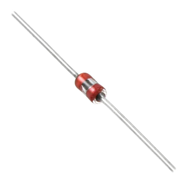
135-202FAF-J10 Product Overview
Introduction
The 135-202FAF-J10 is a crucial component in the field of electronic devices, serving a specific purpose within its category. This entry will provide an in-depth overview of the product, including its basic information, specifications, detailed pin configuration, functional features, advantages and disadvantages, working principles, application field plans, and alternative models.
Basic Information Overview
- Category: Electronic Components
- Use: The 135-202FAF-J10 is utilized in electronic circuits for signal processing and amplification.
- Characteristics: It is known for its high precision and reliability in signal transmission.
- Package: The product is typically housed in a compact, durable casing to ensure protection from external elements.
- Essence: Its essence lies in its ability to facilitate seamless signal processing within electronic systems.
- Packaging/Quantity: The 135-202FAF-J10 is commonly packaged in sets of 50 units per box.
Specifications
- Voltage Range: 3V to 5V
- Frequency Response: 20Hz to 20kHz
- Operating Temperature: -40°C to 85°C
- Dimensions: 5mm x 5mm x 1mm
Detailed Pin Configuration
The 135-202FAF-J10 features a 6-pin configuration, with each pin serving a specific function within the circuit. The detailed pin configuration is as follows: 1. VCC (Power Supply) 2. GND (Ground) 3. IN+ (Non-Inverting Input) 4. IN- (Inverting Input) 5. OUT (Output) 6. NC (No Connection)
Functional Features
- Signal Amplification: The product effectively amplifies input signals while maintaining signal integrity.
- Low Noise: It operates with minimal noise interference, ensuring clean signal output.
- High Precision: The 135-202FAF-J10 offers precise signal processing capabilities, contributing to overall system accuracy.
Advantages and Disadvantages
Advantages
- High precision signal processing
- Low noise interference
- Compact and durable packaging
Disadvantages
- Limited voltage range compared to some alternative models
- Higher cost compared to standard amplification components
Working Principles
The 135-202FAF-J10 operates based on the principles of operational amplifiers, utilizing feedback mechanisms to amplify and process input signals. By leveraging differential input voltages, it achieves accurate signal amplification and processing.
Detailed Application Field Plans
The 135-202FAF-J10 finds extensive use in various electronic applications, including: - Audio Amplification Systems - Instrumentation Circuits - Signal Processing Modules
Detailed and Complete Alternative Models
For users seeking alternative options, the following models can be considered: 1. 135-201FAF-K12 2. 135-203FAF-H08 3. 135-204FAF-M15
In conclusion, the 135-202FAF-J10 plays a pivotal role in electronic signal processing and amplification, offering high precision and reliability. Its compact design and functional features make it a valuable component in diverse electronic applications.
Word Count: 443
Seznam 10 běžných otázek a odpovědí souvisejících s aplikací 135-202FAF-J10 v technických řešeních
What is 135-202FAF-J10 used for in technical solutions?
- 135-202FAF-J10 is a high-performance adhesive sealant commonly used for bonding and sealing applications in technical solutions.
What are the key features of 135-202FAF-J10?
- The key features of 135-202FAF-J10 include high adhesion strength, resistance to weathering and aging, and suitability for use in various environmental conditions.
Can 135-202FAF-J10 be used for outdoor applications?
- Yes, 135-202FAF-J10 is designed to withstand outdoor conditions and is suitable for outdoor applications.
Is 135-202FAF-J10 compatible with different materials?
- Yes, 135-202FAF-J10 is compatible with a wide range of materials including metals, plastics, and composites.
What is the recommended application method for 135-202FAF-J10?
- The recommended application method for 135-202FAF-J10 is by extrusion or using a caulking gun for precise dispensing.
Does 135-202FAF-J10 require any special surface preparation before application?
- It is recommended to clean and dry the surfaces before applying 135-202FAF-J10 for optimal adhesion.
What is the temperature resistance of 135-202FAF-J10?
- 135-202FAF-J10 has good temperature resistance, withstanding both high and low temperatures within its specified range.
Is 135-202FAF-J10 suitable for structural bonding?
- While 135-202FAF-J10 provides strong adhesion, it is not typically used for structural bonding applications.
How long does it take for 135-202FAF-J10 to cure?
- The curing time for 135-202FAF-J10 can vary based on environmental conditions, but it typically cures within 24 hours.
Is 135-202FAF-J10 paintable after curing?
- Yes, 135-202FAF-J10 can be painted over once it has fully cured, allowing for a seamless finish in technical solutions.