Viz Specifikace pro podrobnosti o produktu.

Encyclopedia Entry: 74CBTLV3257PGG8
Product Overview
Category
The 74CBTLV3257PGG8 belongs to the category of integrated circuits (ICs) and specifically falls under the family of multiplexers/demultiplexers.
Use
This IC is primarily used for signal switching applications in electronic circuits. It allows multiple input signals to be routed to a single output or vice versa, enabling efficient data transmission and control.
Characteristics
- Low voltage operation: The 74CBTLV3257PGG8 operates at low voltages, typically between 1.65V and 3.6V, making it suitable for use in battery-powered devices.
- High-speed switching: With a typical propagation delay of only a few nanoseconds, this IC ensures fast and reliable signal routing.
- Wide operating temperature range: The device can operate within a temperature range of -40°C to +85°C, making it suitable for various environmental conditions.
Package
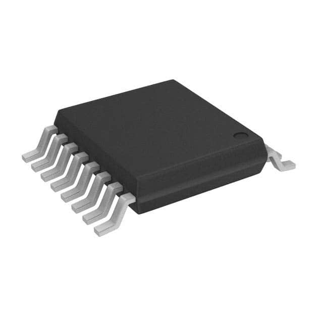
The 74CBTLV3257PGG8 is available in a small form factor package known as TSSOP-16 (Thin Shrink Small Outline Package). This package offers compactness and ease of integration into circuit designs.
Essence
The essence of the 74CBTLV3257PGG8 lies in its ability to efficiently switch signals, allowing for flexible routing and control of data flow within electronic systems.
Packaging/Quantity
The IC is typically supplied in reels or tubes, with each reel containing a quantity of 2500 units. This packaging ensures convenient handling and storage during manufacturing processes.
Specifications
- Number of channels: 4
- Input/output voltage range: 0V to VCC
- On-resistance: 5Ω (typical)
- Supply voltage range: 1.65V to 3.6V
- Maximum operating frequency: 400MHz
Detailed Pin Configuration
The 74CBTLV3257PGG8 features a TSSOP-16 package with the following pin configuration:
___________
      |           |
   1  |1        16| VCC
   2  |2        15| I/O0
   3  |3        14| I/O1
   4  |4        13| I/O2
   5  |5        12| I/O3
   6  |6        11| OE#
   7  |7        10| S
   8  |8         9| GND
      |___________|
Functional Features
- Signal multiplexing/demultiplexing: The IC allows for the selection and routing of input signals to the desired output channel, enabling efficient data transmission.
- Output enable control: The OE# pin enables or disables the outputs, providing flexibility in controlling signal flow.
- Low power consumption: The device is designed to consume minimal power, making it suitable for battery-powered applications.
Advantages and Disadvantages
Advantages
- Compact size and ease of integration into circuit designs.
- Low voltage operation extends battery life in portable devices.
- High-speed switching ensures fast and reliable signal routing.
- Wide operating temperature range allows for versatile usage.
Disadvantages
- Limited number of channels (4) compared to other multiplexer/demultiplexer ICs.
- On-resistance may introduce some signal attenuation.
Working Principles
The 74CBTLV3257PGG8 operates based on the principles of analog multiplexing. It utilizes internal switches controlled by the S pin to connect the desired input signal to the output channel. The OE# pin enables or disables the output, allowing for signal routing or isolation.
Detailed Application Field Plans
The 74CBTLV3257PGG8 finds applications in various fields, including:
- Communication systems: Used for signal routing and switching in telecommunication equipment.
- Data acquisition: Enables multiplexing of sensor signals in data acquisition systems.
- Test and measurement: Facilitates signal routing and control in test equipment.
- Consumer electronics: Utilized in audio/video devices for signal selection and routing.
Detailed and Complete Alternative Models
- SN74CBTLV3257: Similar IC from Texas Instruments with comparable specifications and functionality.
- MC74CBTLV3257: An alternative model offered by ON Semiconductor, providing similar features and performance.
(Note: The above alternative models are provided as examples and may not represent an exhaustive list.)
Word count: 550 words
Seznam 10 běžných otázek a odpovědí souvisejících s aplikací 74CBTLV3257PGG8 v technických řešeních
Sure! Here are 10 common questions and answers related to the application of 74CBTLV3257PGG8 in technical solutions:
Q: What is the function of the 74CBTLV3257PGG8? A: The 74CBTLV3257PGG8 is a quad 2-channel multiplexer/demultiplexer switch used for routing digital signals.
Q: What voltage levels does the 74CBTLV3257PGG8 support? A: The 74CBTLV3257PGG8 supports voltage levels from 1.65V to 3.6V.
Q: How many channels does the 74CBTLV3257PGG8 have? A: The 74CBTLV3257PGG8 has four channels, each with two inputs and one output.
Q: Can the 74CBTLV3257PGG8 be used for bidirectional data transmission? A: Yes, the 74CBTLV3257PGG8 can be used for bidirectional data transmission.
Q: What is the maximum data rate supported by the 74CBTLV3257PGG8? A: The 74CBTLV3257PGG8 supports a maximum data rate of 400 Mbps.
Q: Does the 74CBTLV3257PGG8 have any built-in ESD protection? A: Yes, the 74CBTLV3257PGG8 has built-in ESD protection up to 2kV.
Q: Can the 74CBTLV3257PGG8 be used in hot-swapping applications? A: Yes, the 74CBTLV3257PGG8 is designed to support hot-swapping applications.
Q: What is the power supply voltage range for the 74CBTLV3257PGG8? A: The power supply voltage range for the 74CBTLV3257PGG8 is from 1.65V to 3.6V.
Q: Can the 74CBTLV3257PGG8 be used in both commercial and industrial applications? A: Yes, the 74CBTLV3257PGG8 is suitable for both commercial and industrial applications.
Q: Does the 74CBTLV3257PGG8 have any special features for power management? A: Yes, the 74CBTLV3257PGG8 has a low-power mode that reduces power consumption when not in use.
Please note that these answers are general and may vary depending on the specific application and requirements.

