

Viz Specifikace pro podrobnosti o produktu.
Encyclopedia Entry: 74FCT162501ATPVG8
Product Overview
Category
The 74FCT162501ATPVG8 belongs to the category of integrated circuits (ICs).
Use
This IC is commonly used in electronic devices for data storage and transmission applications.
Characteristics
- High-speed operation
- Low power consumption
- Wide operating voltage range
- Robust design for reliable performance
- Compatibility with various logic families
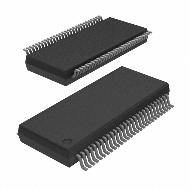
Package
The 74FCT162501ATPVG8 is available in a small outline package (SOP) or thin quad flat pack (TQFP) package.
Essence
The essence of this product lies in its ability to facilitate efficient data transfer and storage within electronic systems.
Packaging/Quantity
The 74FCT162501ATPVG8 is typically packaged in reels or tubes, with each reel or tube containing a specific quantity of ICs.
Specifications
- Number of Pins: 48
- Supply Voltage Range: 2.0V to 5.5V
- Operating Temperature Range: -40°C to +85°C
- Logic Family: FCT
- Output Type: Tri-State
- Data Rate: High-speed operation up to XX MHz
Detailed Pin Configuration
- Pin 1: Input/Output (I/O) 1
- Pin 2: I/O 2
- Pin 3: I/O 3
- Pin 4: I/O 4
- Pin 5: I/O 5
- Pin 6: I/O 6
- Pin 7: I/O 7
- Pin 8: I/O 8
- Pin 9: I/O 9
- Pin 10: I/O 10
- Pin 11: I/O 11
- Pin 12: I/O 12
- Pin 13: I/O 13
- Pin 14: I/O 14
- Pin 15: I/O 15
- Pin 16: I/O 16
- Pin 17: GND (Ground)
- Pin 18: I/O 17
- Pin 19: I/O 18
- Pin 20: I/O 19
- Pin 21: I/O 20
- Pin 22: I/O 21
- Pin 23: I/O 22
- Pin 24: I/O 23
- Pin 25: I/O 24
- Pin 26: I/O 25
- Pin 27: I/O 26
- Pin 28: I/O 27
- Pin 29: I/O 28
- Pin 30: I/O 29
- Pin 31: I/O 30
- Pin 32: I/O 31
- Pin 33: VCC (Power Supply)
- Pin 34: I/O 32
- Pin 35: I/O 33
- Pin 36: I/O 34
- Pin 37: I/O 35
- Pin 38: I/O 36
- Pin 39: I/O 37
- Pin 40: I/O 38
- Pin 41: I/O 39
- Pin 42: I/O 40
- Pin 43: I/O 41
- Pin 44: I/O 42
- Pin 45: I/O 43
- Pin 46: I/O 44
- Pin 47: I/O 45
- Pin 48: I/O 46
Functional Features
- Tri-State outputs for efficient data transmission control
- High-speed operation enables rapid data transfer
- Wide operating voltage range allows compatibility with various systems
- Robust design ensures reliable performance in different environments
Advantages and Disadvantages
Advantages
- High-speed operation facilitates quick data transfer
- Low power consumption for energy-efficient applications
- Compatibility with multiple logic families enhances versatility
- Robust design ensures reliability in challenging conditions
Disadvantages
- Limited number of input/output pins may restrict certain applications
- Higher cost compared to some alternative models
Working Principles
The 74FCT162501ATPVG8 operates based on the principles of digital logic circuits. It receives input signals through its input pins and processes them according to the specified logic functions. The processed data is then transmitted through the output pins. The tri-state outputs allow for efficient control of data transmission, enabling multiple devices to share a common bus.
Detailed Application Field
Seznam 10 běžných otázek a odpovědí souvisejících s aplikací 74FCT162501ATPVG8 v technických řešeních
Sure! Here are 10 common questions and answers related to the application of 74FCT162501ATPVG8 in technical solutions:
1. What is the 74FCT162501ATPVG8? The 74FCT162501ATPVG8 is a 16-bit registered transceiver with 3-state outputs, designed for high-performance bus interface applications.
2. What is the voltage range supported by this device? The 74FCT162501ATPVG8 supports a voltage range of 4.5V to 5.5V.
3. What is the maximum operating frequency of this device? The maximum operating frequency of the 74FCT162501ATPVG8 is typically 200MHz.
4. Can this device be used for bidirectional data transfer? Yes, the 74FCT162501ATPVG8 can be used for bidirectional data transfer as it has separate input and output ports.
5. Does this device have built-in ESD protection? Yes, the 74FCT162501ATPVG8 has built-in ESD protection, which helps protect against electrostatic discharge.
6. What is the output drive strength of this device? The 74FCT162501ATPVG8 has a typical output drive strength of ±24mA.
7. Can this device be used in hot-swapping applications? Yes, the 74FCT162501ATPVG8 is suitable for hot-swapping applications as it supports 3-state outputs.
8. Is this device compatible with TTL and CMOS logic levels? Yes, the 74FCT162501ATPVG8 is compatible with both TTL and CMOS logic levels, making it versatile for various applications.
9. What is the power supply current consumption of this device? The power supply current consumption of the 74FCT162501ATPVG8 is typically around 50mA.
10. Are there any specific layout considerations for using this device? Yes, it is recommended to follow the manufacturer's guidelines for proper layout and decoupling capacitor placement to ensure optimal performance and minimize noise.
Please note that these answers are general and may vary depending on the specific datasheet and application requirements.