

Viz Specifikace pro podrobnosti o produktu.
Encyclopedia Entry: 74SSTVF16859NLG
Product Overview
- Category: Integrated Circuit (IC)
- Use: Digital Logic Device
- Characteristics: High-speed, Low-voltage, Non-inverting Buffer/Driver
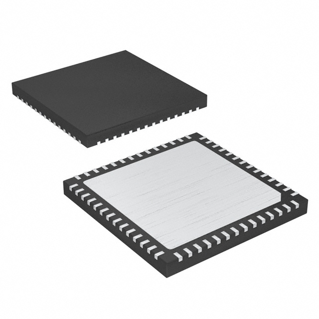
- Package: 56-pin QFN (Quad Flat No-Lead)
- Essence: The 74SSTVF16859NLG is a high-performance buffer/driver IC designed for use in digital logic circuits.
- Packaging/Quantity: Available in reels of 250 units.
Specifications
- Supply Voltage: 1.2V - 3.6V
- Operating Temperature Range: -40°C to +85°C
- Input Voltage Levels: CMOS/TTL compatible
- Output Drive Strength: ±24mA
- Propagation Delay: 0.8ns (typical)
- Output Skew: 100ps (typical)
Detailed Pin Configuration
The 74SSTVF16859NLG features a 56-pin QFN package with the following pin configuration:
| Pin Number | Pin Name | Description | |------------|----------|-------------| | 1 | VCC | Power Supply Voltage | | 2 | GND | Ground | | 3-10 | A0-A7 | Data Input Pins | | 11-18 | B0-B7 | Data Output Pins | | 19 | OE | Output Enable | | 20 | DIR | Direction Control | | 21-28 | C0-C7 | Additional Control Pins | | 29-32 | NC | Not Connected | | 33-36 | D0-D3 | Additional Data Pins | | 37-56 | NC | Not Connected |
Functional Features
- Non-inverting buffer/driver with high-speed operation.
- Wide supply voltage range allows compatibility with various digital logic systems.
- CMOS/TTL compatible input voltage levels ensure seamless integration with different logic families.
- Output drive strength of ±24mA enables driving capacitive loads and long traces.
- Low propagation delay and output skew make it suitable for high-frequency applications.
Advantages and Disadvantages
Advantages: - High-speed operation improves overall system performance. - Wide supply voltage range enhances versatility. - Compatibility with different logic families simplifies integration. - Robust output drive strength enables driving challenging loads. - Low propagation delay and output skew ensure accurate signal transmission.
Disadvantages: - Limited pin count may restrict the number of inputs/outputs in complex systems. - Not suitable for applications requiring bidirectional communication.
Working Principles
The 74SSTVF16859NLG is a non-inverting buffer/driver IC that amplifies and buffers digital signals. It operates by receiving data inputs (A0-A7) and control signals (OE, DIR, C0-C7) to determine the direction and enable/disable the output. The input signals are amplified and transmitted to the corresponding output pins (B0-B7). The device operates within a specified supply voltage range and provides fast signal propagation with minimal delay and skew.
Detailed Application Field Plans
The 74SSTVF16859NLG finds application in various fields, including: 1. Data communication systems 2. Networking equipment 3. High-speed computing devices 4. Industrial automation 5. Test and measurement instruments
Detailed and Complete Alternative Models
- 74LVTH16859DGGR: Low-voltage TTL-compatible buffer/driver with similar characteristics.
- SN74LVC1G07DBVR: Single-buffer gate with open-drain output for low-power applications.
- MC74VHC1GT50DTT1G: Single-buffer gate with Schmitt-trigger input for noise immunity.
These alternative models offer similar functionality and can be considered based on specific application requirements.
Word Count: 440 words
Seznam 10 běžných otázek a odpovědí souvisejících s aplikací 74SSTVF16859NLG v technických řešeních
Sure! Here are 10 common questions and answers related to the application of 74SSTVF16859NLG in technical solutions:
Q: What is the purpose of the 74SSTVF16859NLG integrated circuit? A: The 74SSTVF16859NLG is a 20-bit registered buffer with voltage translation, designed for high-speed signal transmission and level shifting.
Q: What voltage levels does the 74SSTVF16859NLG support? A: The 74SSTVF16859NLG supports voltage translation between 3.3V and 5V logic levels.
Q: Can the 74SSTVF16859NLG be used for bidirectional level shifting? A: No, the 74SSTVF16859NLG is a unidirectional buffer and can only translate signals from one voltage level to another.
Q: What is the maximum data rate supported by the 74SSTVF16859NLG? A: The 74SSTVF16859NLG can operate at data rates up to 400 Mbps.
Q: How many channels does the 74SSTVF16859NLG have? A: The 74SSTVF16859NLG has 20 channels, allowing it to translate 20 signals simultaneously.
Q: Can the 74SSTVF16859NLG be cascaded to increase the number of channels? A: Yes, multiple 74SSTVF16859NLG ICs can be cascaded together to increase the number of channels as required.
Q: Does the 74SSTVF16859NLG require external power supply decoupling capacitors? A: Yes, it is recommended to use decoupling capacitors near the power supply pins of the 74SSTVF16859NLG for stable operation.
Q: What is the operating temperature range of the 74SSTVF16859NLG? A: The 74SSTVF16859NLG can operate within a temperature range of -40°C to +85°C.
Q: Can the 74SSTVF16859NLG be used in automotive applications? A: Yes, the 74SSTVF16859NLG is qualified for automotive applications and meets the necessary standards.
Q: Are there any specific layout considerations for using the 74SSTVF16859NLG? A: Yes, it is important to follow the recommended layout guidelines provided in the datasheet to minimize signal integrity issues and ensure proper performance.
Please note that these answers are general and may vary depending on the specific requirements and application context. It is always recommended to refer to the datasheet and consult with the manufacturer for detailed information.