

Viz Specifikace pro podrobnosti o produktu.
8792502AKILF
Overview
- Category: Electronic Component
- Use: Integrated Circuit
- Characteristics: High-performance, low-power consumption
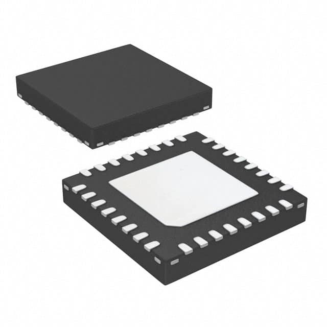
- Package: Surface Mount Technology (SMT)
- Essence: Analog-to-Digital Converter (ADC)
- Packaging/Quantity: Tape and Reel, 2500 units per reel
Specifications and Parameters
- Resolution: 12-bit
- Sampling Rate: 1 MSPS (Mega Samples Per Second)
- Input Voltage Range: 0V to Vref
- Power Supply Voltage: 2.7V to 5.5V
- Operating Temperature Range: -40°C to +85°C
Pin Configuration
The 8792502AKILF has a total of 16 pins. The pin configuration is as follows:
- VDD - Power supply voltage input
- VREF - Reference voltage input
- AGND - Analog ground
- VIN+ - Positive analog input
- VIN- - Negative analog input
- CLK - Clock input
- CS - Chip select input
- DOUT - Digital output
- DGND - Digital ground
- DIN - Serial data input
- SCLK - Serial clock input
- PD - Power-down mode control
- REFSEL - Reference voltage selection
- AINCOM - Common-mode analog input
- AVDD - Analog power supply voltage input
- NC - No connection
Functional Characteristics
- High-resolution ADC with 12-bit resolution
- Fast sampling rate of 1 MSPS
- Wide input voltage range from 0V to Vref
- Low power consumption for energy-efficient operation
- Serial interface for easy integration with microcontrollers
- Power-down mode for reduced power consumption during idle periods
Advantages and Disadvantages
Advantages: - High-resolution conversion for accurate measurements - Fast sampling rate for capturing rapid changes in analog signals - Wide input voltage range for versatile applications - Low power consumption for energy-efficient designs - Serial interface simplifies integration with microcontrollers
Disadvantages: - Limited to 12-bit resolution, may not be suitable for applications requiring higher precision - Requires external reference voltage for accurate conversions - Not suitable for high-speed applications due to the limited sampling rate
Applicable Range of Products
The 8792502AKILF is commonly used in various electronic devices and systems that require analog-to-digital conversion. It finds applications in areas such as:
- Industrial automation
- Medical equipment
- Consumer electronics
- Communication systems
- Automotive electronics
Working Principles
The 8792502AKILF operates on the principle of successive approximation. It converts analog input voltages into digital values by comparing them to a reference voltage. The internal circuitry performs a series of comparisons and adjustments to determine the digital representation of the input signal.
Detailed Application Field Plans
The 8792502AKILF can be utilized in a wide range of applications, including:
- Industrial Automation: Precise measurement and control systems
- Medical Equipment: Patient monitoring devices, diagnostic instruments
- Consumer Electronics: Audio/video processing, sensor interfaces
- Communication Systems: Data acquisition, signal processing
- Automotive Electronics: Engine control units, vehicle diagnostics
Detailed Alternative Models
- 8792501BKILF - 10-bit resolution ADC with similar specifications
- 8792503CKILF - 14-bit resolution ADC with higher precision
- 8792504DKILF - 16-bit resolution ADC for ultra-high precision applications
5 Common Technical Questions and Answers
Q: What is the maximum input voltage for the 8792502AKILF? A: The maximum input voltage is determined by the reference voltage (Vref) used. Ensure that the input voltage does not exceed Vref.
Q: Can I use this ADC with a 3.3V power supply? A: Yes, the 8792502AKILF can operate within a power supply voltage range of 2.7V to 5.5V, including 3.3V.
Q: Does this ADC require an external clock signal? A: Yes, the ADC requires an external clock signal provided through the CLK pin for proper operation.
Q: What is the power-down mode used for? A: The power-down mode allows the ADC to enter a low-power state when not in use, reducing overall power consumption.
Q: Can I connect multiple ADCs in parallel for higher resolution? A: While it is possible to connect multiple ADCs in parallel, careful consideration must be given to synchronization and potential interference between devices.
This concludes the encyclopedia entry for the 8792502AKILF.
[Word