

Viz Specifikace pro podrobnosti o produktu.
IDT71V25761S200PFI
Product Overview
- Category: Integrated Circuit (IC)
- Use: Memory device
- Characteristics: High-speed, low-power, synchronous static random-access memory (SRAM)
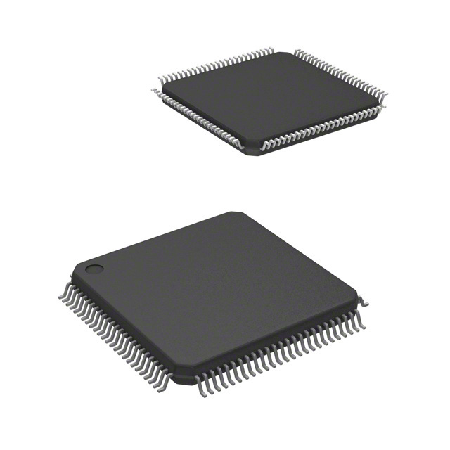
- Package: Plastic Fine-Pitch Ball Grid Array (FBGA)
- Essence: Provides high-performance memory storage for various electronic devices
- Packaging/Quantity: Available in tape and reel packaging, quantity varies based on customer requirements
Specifications
- Memory Type: Synchronous SRAM
- Density: 256K x 36 bits
- Operating Voltage: 2.5V ± 0.2V
- Access Time: 10 ns
- Operating Temperature Range: -40°C to +85°C
- Data Retention: 10 years
- Package Dimensions: 13mm x 13mm
Pin Configuration
The IDT71V25761S200PFI has a total of 100 pins. The pin configuration is as follows:
- VDDQ
- VSSQ
- NC
- DQ0
- DQ1
- DQ2
- DQ3
- DQ4
- DQ5
- DQ6
- DQ7
- DQ8
- DQ9
- DQ10
- DQ11
- DQ12
- DQ13
- DQ14
- DQ15
- DQ16
- DQ17
- DQ18
- DQ19
- DQ20
- DQ21
- DQ22
- DQ23
- DQ24
- DQ25
- DQ26
- DQ27
- DQ28
- DQ29
- DQ30
- DQ31
- VDDQ
- VSSQ
- NC
- A0
- A1
- A2
- A3
- A4
- A5
- A6
- A7
- A8
- A9
- A10
- A11
- A12
- A13
- A14
- A15
- A16
- A17
- A18
- A19
- A20
- A21
- A22
- A23
- A24
- A25
- A26
- A27
- A28
- A29
- A30
- A31
- A32
- A33
- A34
- A35
- A36
- A37
- A38
- A39
- A40
- A41
- A42
- A43
- A44
- A45
- A46
- A47
- A48
- A49
- A50
- A51
- A52
- A53
- A54
- A55
- A56
- A57
- A58
- A59
- A60
- A61
Functional Features
- High-speed operation with a 10 ns access time
- Low-power consumption for energy-efficient applications
- Synchronous interface for easy integration with other components
- Provides reliable and non-volatile storage of data
- Supports simultaneous read and write operations
Advantages and Disadvantages
Advantages: - High-speed performance allows for quick data access - Low-power consumption extends battery life in portable devices - Synchronous interface simplifies system design and integration - Reliable data retention ensures data integrity over time
Disadvantages: - Limited storage capacity compared to other memory technologies - Higher cost per bit compared to alternative memory options - Sensitivity to environmental conditions such as temperature and voltage fluctuations
Working Principles
The IDT71V25761S200PFI is a synchronous SRAM that stores data using flip-flops. It operates based on the principle of synchronous circuitry, where data transfers are synchronized with clock signals. The memory cells are organized into a matrix of rows and columns, allowing for efficient read and write operations. The device uses an internal address decoder to select specific memory locations for data access.
Detailed Application Field Plans
The IDT71
Seznam 10 běžných otázek a odpovědí souvisejících s aplikací IDT71V25761S200PFI v technických řešeních
Sure! Here are 10 common questions and answers related to the application of IDT71V25761S200PFI in technical solutions:
Q: What is the IDT71V25761S200PFI? A: The IDT71V25761S200PFI is a high-speed, low-power, 3.3V CMOS synchronous static RAM (SRAM) with a capacity of 256K x 36.
Q: What are the key features of the IDT71V25761S200PFI? A: Some key features include a synchronous interface, burst mode operation, multiple chip enable options, and a wide operating temperature range.
Q: What is the maximum operating frequency of the IDT71V25761S200PFI? A: The IDT71V25761S200PFI can operate at a maximum frequency of 200 MHz.
Q: Can the IDT71V25761S200PFI be used in battery-powered devices? A: Yes, the IDT71V25761S200PFI is designed to operate at low power, making it suitable for battery-powered devices.
Q: How is the IDT71V25761S200PFI interfaced with other components? A: The IDT71V25761S200PFI uses a synchronous interface, which means it requires a clock signal and control signals to communicate with other components.
Q: Can the IDT71V25761S200PFI be used in industrial applications? A: Yes, the IDT71V25761S200PFI has a wide operating temperature range (-40°C to +85°C), making it suitable for industrial applications.
Q: Does the IDT71V25761S200PFI support burst mode operation? A: Yes, the IDT71V25761S200PFI supports burst mode operation, allowing for efficient data transfer.
Q: What are the different chip enable options available for the IDT71V25761S200PFI? A: The IDT71V25761S200PFI supports multiple chip enable options, including separate chip enables for read and write operations.
Q: Can the IDT71V25761S200PFI be used in high-speed applications? A: Yes, the IDT71V25761S200PFI is a high-speed SRAM with a maximum operating frequency of 200 MHz, making it suitable for high-speed applications.
Q: Are there any specific design considerations when using the IDT71V25761S200PFI? A: Some design considerations include proper power supply decoupling, signal integrity, and ensuring proper timing requirements are met for synchronous operation.
Please note that these answers are general and may vary depending on the specific application and requirements.