

Viz Specifikace pro podrobnosti o produktu.
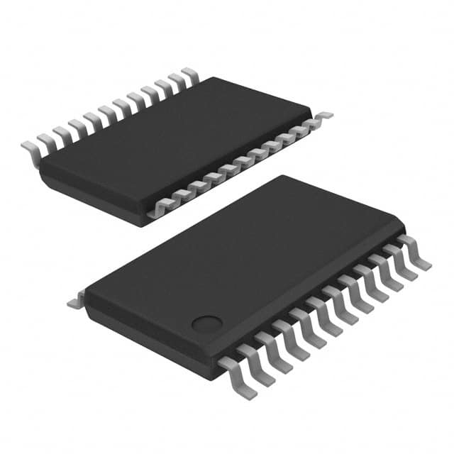
IDT74LVCC3245APGG
Product Overview
- Category: Integrated Circuit (IC)
- Use: Level Shifter/Transceiver
- Characteristics: Bi-directional, 8-bit, non-inverting, tri-state
- Package: 48-pin Thin Quad Flat Pack (TQFP)
- Essence: Transfers data between two different voltage domains
- Packaging/Quantity: Tape and Reel, 250 units per reel
Specifications
- Supply Voltage Range: 2.0V to 3.6V
- Input Voltage Range: 0V to VCC
- Output Voltage Range: 0V to VCC
- Operating Temperature Range: -40°C to +85°C
- Propagation Delay Time: 4.5ns (max)
- Output Drive Capability: ±24mA
- ESD Protection: >2000V (Human Body Model)
Pin Configuration
The IDT74LVCC3245APGG has a total of 48 pins, which are assigned as follows:
- OE (Output Enable) 1
- A1 (Data Bus) 1
- B1 (Data Bus) 1
- GND (Ground)
- B2 (Data Bus) 2
- A2 (Data Bus) 2
- OE (Output Enable) 2
- VCC (Supply Voltage)
- B3 (Data Bus) 3
- A3 (Data Bus) 3
- B4 (Data Bus) 4
- A4 (Data Bus) 4
- B5 (Data Bus) 5
- A5 (Data Bus) 5
- B6 (Data Bus) 6
- A6 (Data Bus) 6
- B7 (Data Bus) 7
- A7 (Data Bus) 7
- B8 (Data Bus) 8
- A8 (Data Bus) 8
- VCC (Supply Voltage)
- GND (Ground)
- DIR (Direction Control)
- OE (Output Enable) 3
- A9 (Data Bus) 9
- B9 (Data Bus) 9
- A10 (Data Bus) 10
- B10 (Data Bus) 10
- A11 (Data Bus) 11
- B11 (Data Bus) 11
- A12 (Data Bus) 12
- B12 (Data Bus) 12
- A13 (Data Bus) 13
- B13 (Data Bus) 13
- A14 (Data Bus) 14
- B14 (Data Bus) 14
- A15 (Data Bus) 15
- B15 (Data Bus) 15
- A16 (Data Bus) 16
- B16 (Data Bus) 16
- GND (Ground)
- VCC (Supply Voltage)
- B17 (Data Bus) 17
- A17 (Data Bus) 17
- B18 (Data Bus) 18
- A18 (Data Bus) 18
- B19 (Data Bus) 19
- A19 (Data Bus) 19
Functional Features
- Bi-directional data transfer between two voltage domains
- Non-inverting logic translation
- Tri-state outputs for bus sharing
- Output enable control for flexible operation
- High-speed operation with low propagation delay
Advantages and Disadvantages
Advantages: - Bi-directional data transfer simplifies system design - Non-inverting logic translation preserves signal integrity - Tri-state outputs allow multiple devices to share a bus - High-speed operation enhances overall system performance
Disadvantages: - Limited voltage range (2.0V to 3.6V) - Propagation delay may impact real-time applications
Working Principles
The IDT74LVCC3245APGG is a level shifter/transceiver IC that facilitates the transfer of data between two different voltage domains. It operates by receiving data from one domain and translating it into a compatible format for the other domain. The non-inverting nature of the device ensures that the logic levels are preserved during translation. The tri-state outputs enable multiple devices to share a common bus, allowing for efficient communication.
Detailed Application Field Plans
The IDT74LVCC3245APGG is commonly used in various applications, including:
- Microcontroller interfacing with different voltage peripherals
- Communication systems involving mixed voltage levels
- Data acquisition systems with multiple voltage domains
- Industrial automation and control systems 5
Seznam 10 běžných otázek a odpovědí souvisejících s aplikací IDT74LVCC3245APGG v technických řešeních
Sure! Here are 10 common questions and answers related to the application of IDT74LVCC3245APGG in technical solutions:
Question: What is the IDT74LVCC3245APGG?
Answer: The IDT74LVCC3245APGG is a bidirectional octal bus transceiver with 3-state outputs.Question: What is the voltage range supported by IDT74LVCC3245APGG?
Answer: The IDT74LVCC3245APGG supports a voltage range of 2.0V to 3.6V.Question: How many bits can the IDT74LVCC3245APGG handle?
Answer: The IDT74LVCC3245APGG can handle 8 bits of data.Question: Can the IDT74LVCC3245APGG be used for level shifting?
Answer: Yes, the IDT74LVCC3245APGG can be used for level shifting between different voltage domains.Question: What is the maximum data transfer rate supported by IDT74LVCC3245APGG?
Answer: The IDT74LVCC3245APGG supports a maximum data transfer rate of 200Mbps.Question: Is the IDT74LVCC3245APGG compatible with TTL logic levels?
Answer: No, the IDT74LVCC3245APGG is not compatible with TTL logic levels. It operates at CMOS logic levels.Question: Can the IDT74LVCC3245APGG be used in both input and output applications?
Answer: Yes, the IDT74LVCC3245APGG can be used as both an input and output buffer.Question: Does the IDT74LVCC3245APGG have built-in ESD protection?
Answer: Yes, the IDT74LVCC3245APGG has built-in ESD protection to prevent damage from electrostatic discharge.Question: What is the power supply voltage required for IDT74LVCC3245APGG?
Answer: The IDT74LVCC3245APGG requires a power supply voltage of 2.0V to 3.6V.Question: Can the IDT74LVCC3245APGG be used in high-speed data communication applications?
Answer: Yes, the IDT74LVCC3245APGG can be used in high-speed data communication applications due to its fast data transfer rate and bidirectional capability.
Please note that these answers are general and may vary depending on the specific application and requirements.