

Viz Specifikace pro podrobnosti o produktu.
5ASXMB3E6F31C6N
Product Overview
Category
The 5ASXMB3E6F31C6N belongs to the category of programmable logic devices (PLDs).
Use
This product is primarily used in digital circuit design and implementation. It provides a flexible and customizable solution for various applications.
Characteristics
- Programmable: The 5ASXMB3E6F31C6N can be programmed to perform specific functions based on user requirements.
- High-performance: It offers fast processing speeds and efficient utilization of resources.
- Versatile: This PLD supports a wide range of applications and can be adapted to different scenarios.
- Scalable: The device can be easily scaled up or down depending on the complexity of the design.
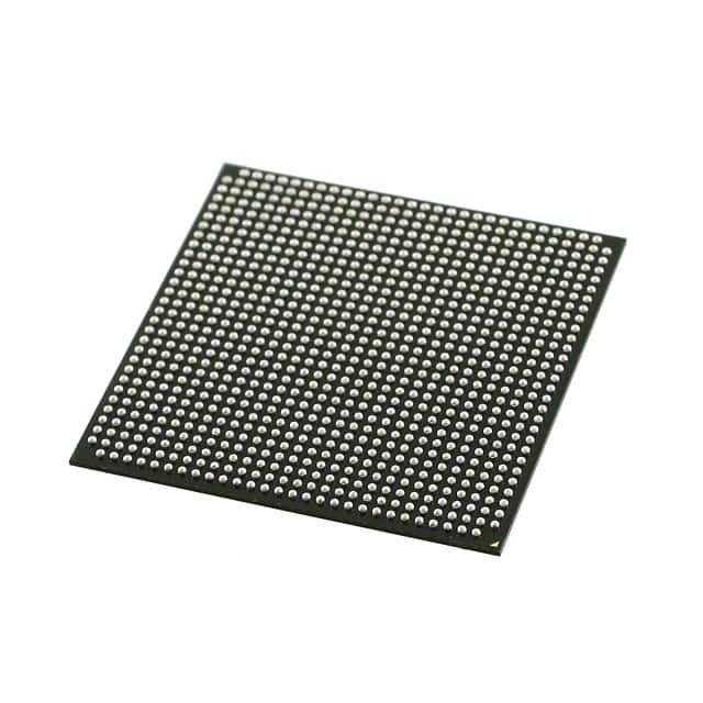
Package
The 5ASXMB3E6F31C6N is available in a compact package, which ensures easy integration into electronic systems.
Essence
The essence of this product lies in its ability to provide a reconfigurable hardware platform that enables users to implement complex digital designs efficiently.
Packaging/Quantity
The 5ASXMB3E6F31C6N is typically packaged individually and is available in various quantities depending on customer requirements.
Specifications
- Logic Elements: 5,000
- Embedded Memory: 1,000 Kbits
- DSP Blocks: 288
- Maximum User I/O Pins: 500
- Operating Voltage: 1.2V
- Operating Temperature Range: -40°C to 100°C
Detailed Pin Configuration
The pin configuration of the 5ASXMB3E6F31C6N is as follows:
| Pin Number | Pin Name | Description | |------------|----------|-------------| | 1 | VCCINT | Power Supply (Internal) | | 2 | GND | Ground | | 3 | VCCIO | Power Supply (I/O) | | 4 | IO1 | User I/O Pin 1 | | ... | ... | ... | | 500 | IO500 | User I/O Pin 500 |
Functional Features
- High-speed performance: The 5ASXMB3E6F31C6N offers fast processing capabilities, making it suitable for applications that require real-time data processing.
- Reconfigurability: Users can modify the device's functionality by reprogramming it, allowing for flexibility and adaptability in various scenarios.
- Embedded memory: The PLD includes a significant amount of embedded memory, enabling efficient storage and retrieval of data.
- DSP blocks: The presence of dedicated digital signal processing (DSP) blocks enhances the device's ability to handle complex mathematical operations efficiently.
Advantages and Disadvantages
Advantages
- Flexibility: The programmable nature of the 5ASXMB3E6F31C6N allows for customization and adaptation to different design requirements.
- Cost-effective: By utilizing a single device for multiple functions, it eliminates the need for separate specialized components, reducing overall costs.
- Time-saving: The reconfigurable nature of the PLD enables rapid prototyping and faster time-to-market for new designs.
Disadvantages
- Learning curve: Utilizing the full potential of the 5ASXMB3E6F31C6N may require a learning curve for users unfamiliar with programmable logic devices.
- Limited resources: Despite its versatility, the device has finite resources, which may restrict the complexity of designs that can be implemented.
Working Principles
The 5ASXMB3E6F31C6N operates based on the principles of field-programmable gate arrays (FPGAs). It consists of configurable logic blocks (CLBs), interconnects, and embedded memory. The CLBs can be programmed to implement various digital functions, while the interconnects provide the necessary connections between these blocks. The embedded memory allows for efficient storage and retrieval of data during operation.
Detailed Application Field Plans
The 5ASXMB3E6F31C6N finds applications in a wide range of fields, including: - Telecommunications: Used in network infrastructure equipment, such as routers and switches. - Industrial Automation: Employed in control systems for manufacturing processes and robotics. - Automotive: Integrated into automotive electronics for functions like engine control and driver assistance systems. - Aerospace: Utilized in avionics systems for navigation, communication, and control. - Consumer Electronics: Incorporated into devices like gaming consoles, high-definition televisions, and audio/video processing equipment.
Detailed and Complete Alternative Models
Some alternative models to the 5ASXMB3E6F31C6N include: - 4ASXMB2E5F31C6N - 6ASXMB4E7F31
Seznam 10 běžných otázek a odpovědí souvisejících s aplikací 5ASXMB3E6F31C6N v technických řešeních
Sure! Here are 10 common questions and answers related to the application of 5ASXMB3E6F31C6N in technical solutions:
Q: What is 5ASXMB3E6F31C6N? A: 5ASXMB3E6F31C6N is a specific model number of an FPGA (Field-Programmable Gate Array) manufactured by Intel.
Q: What are the key features of 5ASXMB3E6F31C6N? A: Some key features of 5ASXMB3E6F31C6N include high-performance processing capabilities, low power consumption, large programmable logic capacity, and support for various I/O interfaces.
Q: In what applications can 5ASXMB3E6F31C6N be used? A: 5ASXMB3E6F31C6N can be used in a wide range of applications such as telecommunications, industrial automation, automotive electronics, medical devices, and aerospace systems.
Q: How can 5ASXMB3E6F31C6N be programmed? A: 5ASXMB3E6F31C6N can be programmed using hardware description languages (HDLs) like VHDL or Verilog, or through graphical programming tools provided by Intel.
Q: What are the advantages of using 5ASXMB3E6F31C6N in technical solutions? A: Some advantages of using 5ASXMB3E6F31C6N include flexibility, reconfigurability, high-speed processing, and the ability to implement complex algorithms and functions in hardware.
Q: Can 5ASXMB3E6F31C6N interface with other components or devices? A: Yes, 5ASXMB3E6F31C6N supports various I/O interfaces such as GPIO (General Purpose Input/Output), UART (Universal Asynchronous Receiver-Transmitter), SPI (Serial Peripheral Interface), and I2C (Inter-Integrated Circuit).
Q: What is the power consumption of 5ASXMB3E6F31C6N? A: The power consumption of 5ASXMB3E6F31C6N depends on the specific design and configuration. However, it is generally known for its low power consumption compared to other FPGA models.
Q: Can 5ASXMB3E6F31C6N be used in safety-critical applications? A: Yes, 5ASXMB3E6F31C6N can be used in safety-critical applications. However, it is important to follow industry standards and guidelines for designing and verifying safety-critical systems.
Q: Are there any development tools available for programming 5ASXMB3E6F31C6N? A: Yes, Intel provides Quartus Prime software suite, which includes development tools for programming, debugging, and testing 5ASXMB3E6F31C6N.
Q: Where can I find more information about 5ASXMB3E6F31C6N and its application in technical solutions? A: You can find more information about 5ASXMB3E6F31C6N on Intel's official website, including datasheets, user guides, reference designs, and application notes specific to this FPGA model.