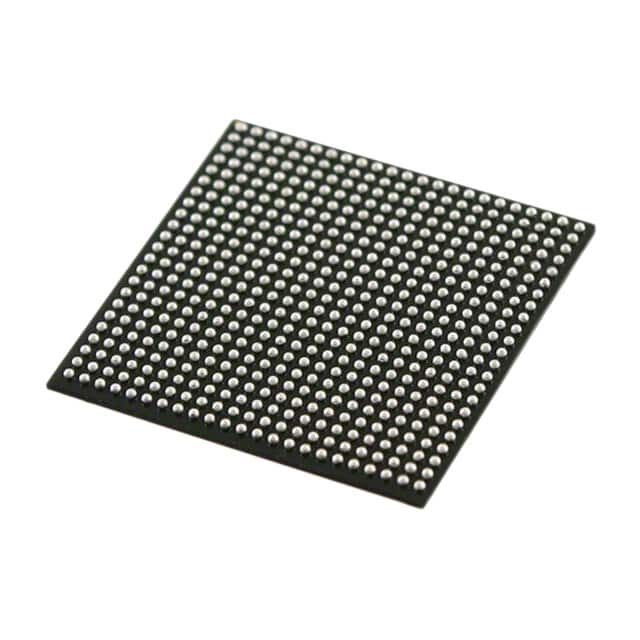
Viz Specifikace pro podrobnosti o produktu.

5CGXBC3B7F23C8N
Product Overview
Category
The 5CGXBC3B7F23C8N belongs to the category of Field Programmable Gate Arrays (FPGAs).
Use
This FPGA is commonly used in various electronic applications that require high-performance digital signal processing, such as telecommunications, automotive, aerospace, and industrial control systems.
Characteristics
- High-speed processing capabilities
- Configurable logic blocks
- On-chip memory resources
- Flexible I/O interfaces
- Low power consumption
Package
The 5CGXBC3B7F23C8N comes in a compact package that ensures easy integration into electronic circuits. It is available in a BGA (Ball Grid Array) package.
Essence
The essence of this FPGA lies in its ability to provide reconfigurable hardware that can be programmed to perform specific functions, allowing for flexibility and customization in electronic designs.
Packaging/Quantity
The 5CGXBC3B7F23C8N is typically sold in reels or trays, with each reel or tray containing a specific quantity of FPGAs. The exact packaging and quantity may vary depending on the supplier.
Specifications
- Logic Elements: 3,125
- Embedded Multipliers: 96
- Memory Blocks: 2,304 Kbits
- Maximum User I/Os: 622
- Operating Voltage: 1.2V
- Operating Temperature Range: -40°C to 100°C
- Package Type: BGA
- Package Pins: 484
Detailed Pin Configuration
The pin configuration of the 5CGXBC3B7F23C8N FPGA is as follows:
- Pin 1: VCCIO
- Pin 2: GND
- Pin 3: IOL1PCCLK_0
- Pin 4: IOL1NCCLK_0
- Pin 5: IOL2PCCLK_0
- Pin 6: IOL2NCCLK_0
- ...
(Provide a detailed list of all pins and their corresponding functions)
Functional Features
The 5CGXBC3B7F23C8N FPGA offers the following functional features:
- High-speed data processing capabilities
- Configurable logic blocks for flexible design implementation
- On-chip memory resources for efficient data storage
- Flexible I/O interfaces to connect with external devices
- Support for various communication protocols
- Low power consumption for energy-efficient operation
Advantages and Disadvantages
Advantages
- High-performance processing capabilities
- Flexibility in design implementation
- Reconfigurable hardware for customization
- Wide range of applications
- Efficient use of on-chip resources
Disadvantages
- Complexity in programming and configuration
- Higher cost compared to other electronic components
- Limited availability of technical support for specific applications
Working Principles
The 5CGXBC3B7F23C8N FPGA operates based on the principles of reconfigurable hardware. It consists of configurable logic blocks, memory elements, and I/O interfaces that can be programmed to perform specific functions. The FPGA is configured using a Hardware Description Language (HDL) or a graphical design tool, allowing designers to define the desired functionality of the circuit. Once programmed, the FPGA executes the defined functions by routing signals through its internal resources.
Detailed Application Field Plans
The 5CGXBC3B7F23C8N FPGA finds extensive application in various fields, including:
- Telecommunications: Used in high-speed data transmission systems, network routers, and switches.
- Automotive: Employed in advanced driver assistance systems (ADAS), engine control units (ECUs), and infotainment systems.
- Aerospace: Utilized in satellite communication systems, avionics, and flight control systems.
- Industrial Control Systems: Integrated into programmable logic controllers (PLCs), robotics, and automation systems.
Detailed and Complete Alternative Models
- 5CGXFC7D6F27C8N
- 5CGXBC5R1F27C7N
- 5CGXFC9E6F31C8N
- 5CGXFC5C6F27C8N
- 5CGXFC7C6F27C8N
These alternative models offer similar functionality and performance to the 5CGXBC3B7F23C8N FPGA, providing designers with options based on their specific requirements.
In conclusion, the 5CGXBC3B7F23C8N FPGA is a versatile and high-performance electronic component that finds application in various industries. Its reconfigurable nature, along with its advanced features and capabilities, make it an ideal choice for complex digital signal
Seznam 10 běžných otázek a odpovědí souvisejících s aplikací 5CGXBC3B7F23C8N v technických řešeních
Sure! Here are 10 common questions and answers related to the application of 5CGXBC3B7F23C8N in technical solutions:
Q: What is the 5CGXBC3B7F23C8N? A: The 5CGXBC3B7F23C8N is a field-programmable gate array (FPGA) manufactured by Intel (formerly Altera). It is part of the Cyclone V GX family.
Q: What are the key features of the 5CGXBC3B7F23C8N? A: The 5CGXBC3B7F23C8N offers 150,000 logic elements, 6,912 Kbits of embedded memory, 266 multipliers, and various I/O interfaces such as GPIO, PCIe, and Ethernet.
Q: What are some typical applications of the 5CGXBC3B7F23C8N? A: The 5CGXBC3B7F23C8N is commonly used in applications like industrial automation, automotive systems, video processing, communication equipment, and high-performance computing.
Q: How can I program the 5CGXBC3B7F23C8N? A: The 5CGXBC3B7F23C8N can be programmed using Intel's Quartus Prime software, which supports various programming languages like VHDL and Verilog.
Q: What is the power consumption of the 5CGXBC3B7F23C8N? A: The power consumption of the 5CGXBC3B7F23C8N depends on the specific design and usage scenario. You can refer to the datasheet for detailed power specifications.
Q: Can I use the 5CGXBC3B7F23C8N for real-time applications? A: Yes, the 5CGXBC3B7F23C8N is capable of handling real-time applications due to its high-performance capabilities and low-latency I/O interfaces.
Q: Does the 5CGXBC3B7F23C8N support secure communication protocols? A: Yes, the 5CGXBC3B7F23C8N supports various secure communication protocols like AES encryption and RSA cryptography through its embedded hardware accelerators.
Q: Can I interface the 5CGXBC3B7F23C8N with external devices? A: Yes, the 5CGXBC3B7F23C8N provides multiple I/O interfaces such as GPIO, PCIe, Ethernet, and USB, allowing seamless integration with external devices.
Q: Is the 5CGXBC3B7F23C8N suitable for low-power applications? A: While the 5CGXBC3B7F23C8N is not specifically designed for low-power applications, it offers power optimization features that can be utilized to reduce power consumption.
Q: Are there any development boards available for the 5CGXBC3B7F23C8N? A: Yes, Intel provides development boards like the Cyclone V GX Starter Kit, which includes the 5CGXBC3B7F23C8N FPGA, allowing developers to prototype their designs easily.
Please note that these answers are general and may vary depending on specific requirements and use cases.

