

Viz Specifikace pro podrobnosti o produktu.
5CGXBC4C6F27C7N
Product Overview
Category
The 5CGXBC4C6F27C7N belongs to the category of Field Programmable Gate Arrays (FPGAs).
Use
FPGAs are integrated circuits that can be programmed after manufacturing. They are widely used in various electronic applications, including telecommunications, automotive, aerospace, and consumer electronics.
Characteristics
- The 5CGXBC4C6F27C7N is a high-performance FPGA with advanced features.
- It offers a large number of programmable logic elements, allowing for complex digital designs.
- The device supports high-speed interfaces and has built-in memory blocks for efficient data processing.
- It provides flexibility in design iterations and reduces time-to-market for electronic products.
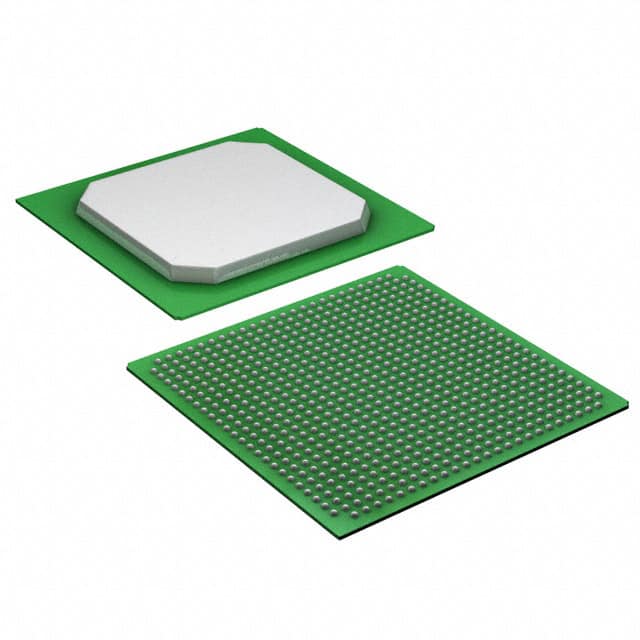
Package
The 5CGXBC4C6F27C7N comes in a compact package suitable for surface mount technology (SMT) assembly. The package ensures easy integration into electronic systems and provides protection against environmental factors.
Essence
The essence of the 5CGXBC4C6F27C7N lies in its ability to provide reconfigurable hardware resources, enabling designers to implement custom logic functions and algorithms.
Packaging/Quantity
The 5CGXBC4C6F27C7N is typically packaged in trays or reels, depending on the manufacturer's specifications. The quantity per package varies but is commonly available in quantities of 100 or more.
Specifications
- Logic Elements: 4,600
- Embedded Memory: 2,073,600 bits
- Maximum User I/Os: 622
- Clock Management Tiles: 8
- DSP Blocks: 96
- Maximum Operating Frequency: 500 MHz
- Operating Voltage: 1.2V
- Package Type: BGA (Ball Grid Array)
- Package Pins: 484
Detailed Pin Configuration
The 5CGXBC4C6F27C7N has a total of 484 pins, each serving a specific purpose in the FPGA's functionality. The pin configuration includes input/output pins, power supply pins, clock pins, and configuration pins. A detailed pinout diagram is available in the product datasheet.
Functional Features
High-Speed Interfaces
The 5CGXBC4C6F27C7N supports various high-speed interfaces, including PCIe, Gigabit Ethernet, DDR3 memory, and USB. This enables seamless integration with other electronic components and facilitates fast data transfer rates.
Reconfigurable Logic
The FPGA's reconfigurable logic allows designers to modify the hardware functionality even after manufacturing. This flexibility enables rapid prototyping, design iterations, and customization for specific applications.
Embedded Memory Blocks
The device incorporates a significant amount of embedded memory blocks, providing efficient storage for data processing. These memory blocks can be used as RAM, ROM, or FIFO buffers, enhancing the overall performance of the FPGA.
Clock Management Tiles
The presence of clock management tiles simplifies the generation and distribution of clock signals within the FPGA. It ensures precise timing control and synchronization, critical for complex digital designs.
Advantages and Disadvantages
Advantages
- Flexibility in design iterations and customization.
- High-performance capabilities for complex digital designs.
- Support for various high-speed interfaces.
- Efficient use of embedded memory resources.
- Precise timing control with clock management tiles.
Disadvantages
- Steep learning curve for beginners due to the complexity of FPGA programming.
- Higher cost compared to traditional fixed-function integrated circuits.
- Power consumption can be relatively high, especially for resource-intensive designs.
Working Principles
The 5CGXBC4C6F27C7N operates based on the principles of reconfigurable hardware. It consists of a matrix of programmable logic elements interconnected through configurable routing resources. The device can be programmed using Hardware Description Languages (HDLs) such as VHDL or Verilog, which describe the desired functionality of the FPGA.
During operation, the FPGA's configuration memory is loaded with the user-defined bitstream, which determines the interconnections and behavior of the logic elements. The FPGA then executes the programmed logic, performing various digital operations based on the input signals and internal state.
Detailed Application Field Plans
The 5CGXBC4C6F27C7N finds applications in a wide range of fields, including:
- Telecommunications: Used in base stations, routers, and network switches for high-speed data processing and protocol handling.
- Automotive: Employed in advanced driver-assistance systems (ADAS), infotainment systems, and engine control units (ECUs) for real-time data processing and control.
- Aerospace: Utilized in avionics systems, satellite communication, and radar systems for reliable and high-performance signal processing.
- Consumer Electronics: Integrated into smart TVs,
Seznam 10 běžných otázek a odpovědí souvisejících s aplikací 5CGXBC4C6F27C7N v technických řešeních
Sure! Here are 10 common questions and answers related to the application of 5CGXBC4C6F27C7N in technical solutions:
Q: What is the 5CGXBC4C6F27C7N FPGA used for? A: The 5CGXBC4C6F27C7N is a field-programmable gate array (FPGA) that can be used for various applications such as digital signal processing, high-speed communication, and embedded systems.
Q: What are the key features of the 5CGXBC4C6F27C7N FPGA? A: Some key features include a high logic density, low power consumption, high-speed transceivers, embedded memory blocks, and support for various I/O standards.
Q: Can the 5CGXBC4C6F27C7N FPGA be reprogrammed? A: Yes, the 5CGXBC4C6F27C7N is a field-programmable device, which means it can be reprogrammed multiple times to implement different functionalities or designs.
Q: What tools are available for programming the 5CGXBC4C6F27C7N FPGA? A: Intel Quartus Prime is the primary software tool used for designing, programming, and debugging the 5CGXBC4C6F27C7N FPGA. It provides a comprehensive development environment.
Q: What are the advantages of using an FPGA like 5CGXBC4C6F27C7N over other types of integrated circuits? A: FPGAs offer flexibility, allowing designers to implement custom logic functions and algorithms. They also provide high performance, parallel processing capabilities, and can be reconfigured as needed.
Q: Can the 5CGXBC4C6F27C7N FPGA interface with other components or devices? A: Yes, the FPGA has various I/O standards and interfaces such as LVDS, DDR3 memory controllers, PCIe, Ethernet, and more, making it compatible with a wide range of components and devices.
Q: What is the power consumption of the 5CGXBC4C6F27C7N FPGA? A: The power consumption of the FPGA depends on the design and utilization. However, it is designed to be power-efficient, and power optimization techniques can be applied during the design process.
Q: Are there any development boards available for prototyping with the 5CGXBC4C6F27C7N FPGA? A: Yes, Intel provides development kits and evaluation boards that include the 5CGXBC4C6F27C7N FPGA, allowing engineers to prototype and test their designs before production.
Q: Can the 5CGXBC4C6F27C7N FPGA be used in safety-critical applications? A: Yes, the 5CGXBC4C6F27C7N FPGA can be used in safety-critical applications. However, additional measures such as redundancy, fault tolerance, and rigorous testing may be required to meet safety standards.
Q: Where can I find documentation and support for the 5CGXBC4C6F27C7N FPGA? A: Intel provides comprehensive documentation, datasheets, application notes, and technical support for the 5CGXBC4C6F27C7N FPGA on their official website. Additionally, online forums and communities can also provide valuable resources and support.