

Viz Specifikace pro podrobnosti o produktu.
5CGXBC5C7F27C8N
Product Overview
Category
The 5CGXBC5C7F27C8N belongs to the category of Field Programmable Gate Arrays (FPGAs).
Use
FPGAs are integrated circuits that can be programmed and reprogrammed to perform various digital functions. The 5CGXBC5C7F27C8N is specifically designed for high-performance applications.
Characteristics
- High-performance FPGA with advanced features
- Large capacity and high-speed processing capabilities
- Flexible and reconfigurable design
- Low power consumption
- Robust and reliable performance
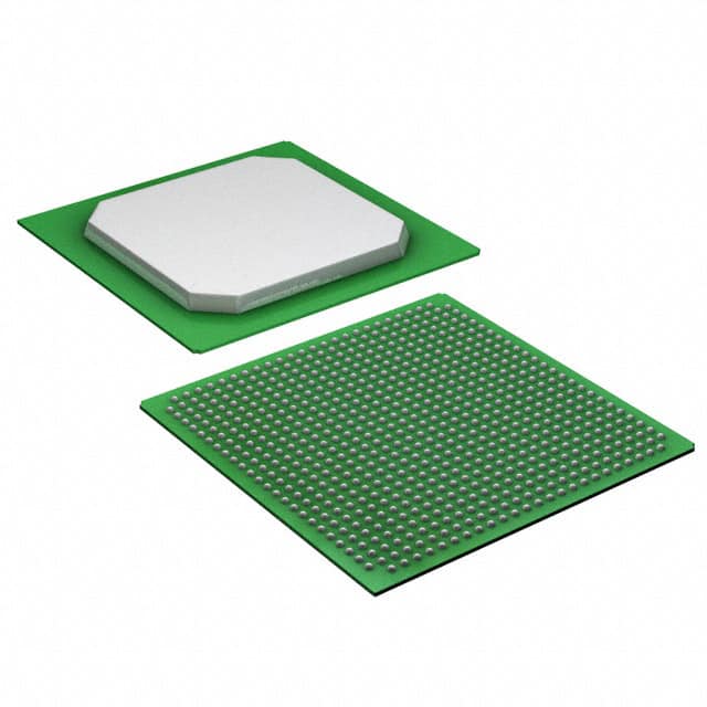
Package
The 5CGXBC5C7F27C8N comes in a compact package, suitable for easy integration into electronic systems.
Essence
The essence of the 5CGXBC5C7F27C8N lies in its ability to provide a versatile and powerful platform for implementing complex digital designs.
Packaging/Quantity
The 5CGXBC5C7F27C8N is typically packaged individually and is available in various quantities depending on the customer's requirements.
Specifications
- FPGA Family: Cyclone V GX
- Logic Elements: 77,580
- Embedded Memory: 3,888 Kbits
- Maximum User I/Os: 622
- DSP Blocks: 352
- Maximum Operating Frequency: 300 MHz
- Voltage Supply: 1.2V
Detailed Pin Configuration
The 5CGXBC5C7F27C8N has a comprehensive pin configuration, allowing for connectivity with external devices and components. Please refer to the datasheet for the detailed pinout information.
Functional Features
- High-speed data processing capabilities
- Support for various communication protocols
- On-chip memory resources for efficient data storage
- Configurable I/O standards for easy interfacing with external devices
- Built-in digital signal processing blocks for complex algorithms
Advantages and Disadvantages
Advantages
- Versatile and flexible design for a wide range of applications
- High-performance capabilities suitable for demanding tasks
- Low power consumption for energy-efficient operation
- Robust and reliable performance in harsh environments
Disadvantages
- Steep learning curve for beginners due to the complexity of FPGA programming
- Higher cost compared to other programmable logic devices
- Limited availability of alternative models with similar specifications
Working Principles
The 5CGXBC5C7F27C8N operates based on the principles of reconfigurable logic. It consists of an array of configurable logic blocks interconnected through programmable routing resources. The user can program the FPGA to implement desired digital functions by configuring the interconnections and functionality of these logic blocks.
Detailed Application Field Plans
The 5CGXBC5C7F27C8N finds applications in various fields, including:
- Telecommunications: Used in high-speed data transmission systems, network routers, and switches.
- Aerospace and Defense: Employed in radar systems, avionics, and military communication equipment.
- Industrial Automation: Utilized in control systems, robotics, and machine vision applications.
- Medical Devices: Integrated into medical imaging systems, patient monitoring devices, and diagnostic equipment.
- Automotive: Applied in advanced driver assistance systems (ADAS), infotainment systems, and engine control units.
Detailed and Complete Alternative Models
While the 5CGXBC5C7F27C8N offers exceptional features, there are alternative FPGA models available in the market that cater to different requirements. Some notable alternatives include:
- Xilinx Virtex UltraScale+: Offers higher logic capacity and performance for demanding applications.
- Intel Stratix 10: Provides advanced features and scalability for complex designs.
- Lattice ECP5: Focuses on low power consumption and small form factor applications.
These alternative models offer different trade-offs in terms of performance, power consumption, and cost, allowing users to choose the most suitable FPGA for their specific needs.
Word count: 550 words
Seznam 10 běžných otázek a odpovědí souvisejících s aplikací 5CGXBC5C7F27C8N v technických řešeních
Sure! Here are 10 common questions and answers related to the application of 5CGXBC5C7F27C8N in technical solutions:
Q: What is the 5CGXBC5C7F27C8N FPGA used for? A: The 5CGXBC5C7F27C8N is a Field-Programmable Gate Array (FPGA) that can be used for various applications such as digital signal processing, high-speed communication, and embedded systems.
Q: What is the maximum number of logic elements in the 5CGXBC5C7F27C8N? A: The 5CGXBC5C7F27C8N FPGA has a maximum of 5,760 logic elements (LEs).
Q: Can the 5CGXBC5C7F27C8N support high-speed communication protocols? A: Yes, the 5CGXBC5C7F27C8N FPGA supports high-speed communication protocols like PCIe, Ethernet, and USB.
Q: Does the 5CGXBC5C7F27C8N have built-in memory blocks? A: Yes, the 5CGXBC5C7F27C8N FPGA has embedded memory blocks called M20K blocks that can be used for storing data.
Q: What is the maximum number of multipliers available in the 5CGXBC5C7F27C8N? A: The 5CGXBC5C7F27C8N FPGA has a maximum of 288 variable-precision DSP blocks, which can be used as multipliers.
Q: Can I use the 5CGXBC5C7F27C8N for video processing applications? A: Yes, the 5CGXBC5C7F27C8N FPGA can be used for video processing applications like image filtering, video compression, and real-time video analytics.
Q: What is the maximum number of I/O pins available in the 5CGXBC5C7F27C8N? A: The 5CGXBC5C7F27C8N FPGA has a maximum of 622 I/O pins, which can be used for interfacing with external devices.
Q: Can I reprogram the 5CGXBC5C7F27C8N after it has been configured? A: Yes, the 5CGXBC5C7F27C8N FPGA is field-programmable, meaning you can reprogram it multiple times to implement different designs.
Q: Does the 5CGXBC5C7F27C8N support partial reconfiguration? A: Yes, the 5CGXBC5C7F27C8N FPGA supports partial reconfiguration, allowing you to modify specific sections of the design without reprogramming the entire device.
Q: What development tools are available for programming the 5CGXBC5C7F27C8N? A: The 5CGXBC5C7F27C8N FPGA can be programmed using Intel Quartus Prime software, which provides a comprehensive development environment for designing and configuring FPGAs.
Please note that the answers provided here are general and may vary depending on the specific requirements and configurations of your technical solution.