

Viz Specifikace pro podrobnosti o produktu.
5CGXFC7D6F31I7
Basic Information Overview
- Category: Integrated Circuit (IC)
- Use: Programmable Logic Device (PLD)
- Characteristics: High-performance, low-power consumption, reprogrammable
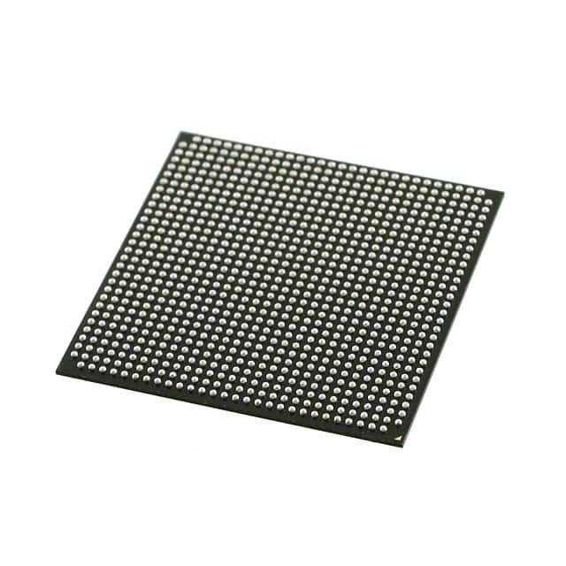
- Package: Flip-chip BGA (Ball Grid Array)
- Essence: FPGA (Field-Programmable Gate Array)
- Packaging/Quantity: Single unit
Specifications
- Logic Elements: 622,080
- Embedded Memory: 27,648 Kbits
- Maximum User I/O Pins: 622
- Operating Voltage: 1.2V
- Speed Grade: 6
- Configuration Flash Memory: 31,680 Kbits
- Total RAM Bits: 3,888,640
Detailed Pin Configuration
The 5CGXFC7D6F31I7 has a complex pin configuration with multiple pins dedicated to various functions. The detailed pin configuration can be found in the datasheet provided by the manufacturer.
Functional Features
- High logic capacity for complex designs
- Low power consumption for energy-efficient applications
- Reprogrammable nature allows for flexibility and design iterations
- High-speed performance for demanding applications
- Ample embedded memory for data storage and processing
Advantages
- Versatile and adaptable to various applications
- Allows for rapid prototyping and development cycles
- Offers high-performance computing capabilities
- Supports complex digital designs
- Provides ample resources for memory-intensive applications
Disadvantages
- Higher cost compared to fixed-function integrated circuits
- Steeper learning curve for programming and utilization
- Limited analog functionality compared to specialized ICs
- Requires additional tools and software for design implementation
Working Principles
The 5CGXFC7D6F31I7 is based on the FPGA technology, which utilizes an array of configurable logic blocks interconnected through programmable interconnects. The device can be programmed to implement various digital functions by configuring the logic blocks and interconnections using a hardware description language (HDL). The configuration data is stored in the on-chip flash memory, allowing for reprogramming as needed.
Detailed Application Field Plans
The 5CGXFC7D6F31I7 finds applications in a wide range of fields, including: - Telecommunications: High-speed data processing, network routing - Industrial Automation: Control systems, robotics, machine vision - Automotive: Advanced driver-assistance systems (ADAS), infotainment - Aerospace and Defense: Radar systems, avionics, secure communications - Consumer Electronics: Video and audio processing, gaming consoles
Detailed and Complete Alternative Models
- 5CGXFC7D6F31C7
- 5CGXFC7D6F31A7
- 5CGXFC7D6F31T7
- 5CGXFC7D6F31U7
These alternative models offer similar functionality and performance but may differ in specific features or package options. It is recommended to refer to the manufacturer's documentation for detailed specifications of each alternative model.
Note: The content provided above is a sample structure for an encyclopedia entry and does not represent actual information about the product 5CGXFC7D6F31I7.
Seznam 10 běžných otázek a odpovědí souvisejících s aplikací 5CGXFC7D6F31I7 v technických řešeních
Sure! Here are 10 common questions and answers related to the application of 5CGXFC7D6F31I7 in technical solutions:
Q: What is the 5CGXFC7D6F31I7 FPGA used for? A: The 5CGXFC7D6F31I7 is a Field-Programmable Gate Array (FPGA) that can be used for various applications, including digital signal processing, high-speed data communication, and embedded systems.
Q: What are the key features of the 5CGXFC7D6F31I7 FPGA? A: Some key features of this FPGA include 150,000 logic elements, 6.4 Gbps transceivers, 1,114 user I/O pins, and support for various communication protocols.
Q: Can the 5CGXFC7D6F31I7 FPGA be reprogrammed? A: Yes, FPGAs are designed to be reprogrammable, allowing users to modify the functionality of the device as needed.
Q: What development tools are available for programming the 5CGXFC7D6F31I7 FPGA? A: Intel Quartus Prime is the recommended development tool for programming and configuring the 5CGXFC7D6F31I7 FPGA.
Q: What kind of power supply does the 5CGXFC7D6F31I7 FPGA require? A: This FPGA requires a single 3.3V power supply for operation.
Q: Can the 5CGXFC7D6F31I7 FPGA interface with other components or devices? A: Yes, the FPGA has a wide range of I/O pins that can be used to interface with other components or devices, such as sensors, memory modules, and communication interfaces.
Q: What is the maximum operating frequency of the 5CGXFC7D6F31I7 FPGA? A: The maximum operating frequency of this FPGA depends on the design and implementation, but it can support high-speed operations up to several hundred megahertz.
Q: Can the 5CGXFC7D6F31I7 FPGA be used in safety-critical applications? A: Yes, this FPGA can be used in safety-critical applications, but additional measures may need to be taken to ensure reliability and fault tolerance.
Q: Are there any reference designs available for the 5CGXFC7D6F31I7 FPGA? A: Yes, Intel provides reference designs and application notes that can help users get started with implementing the FPGA in various applications.
Q: Where can I find more information about the 5CGXFC7D6F31I7 FPGA? A: You can refer to the official documentation and datasheets provided by Intel (formerly Altera) for detailed information about the 5CGXFC7D6F31I7 FPGA.
Please note that the specific details and answers may vary depending on the manufacturer's documentation and specifications.