

Viz Specifikace pro podrobnosti o produktu.
5SGSMD3H3F35C2LN
Basic Information Overview
- Category: Integrated Circuit (IC)
- Use: Programmable Logic Device (PLD)
- Characteristics:
- High-performance FPGA (Field-Programmable Gate Array)
- Advanced features for complex digital designs
- Low power consumption
- Large capacity for logic and memory resources
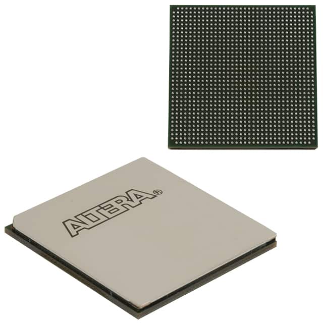
- Package: BGA (Ball Grid Array)
- Essence: Versatile and powerful programmable logic solution
- Packaging/Quantity: Typically sold individually or in small quantities
Specifications
- Manufacturer: Intel Corporation
- Family: Stratix V
- Device Type: FPGA
- Series: 5SGSMD3H3F35C2LN
- Number of Logic Elements: 358,400
- Number of Memory Bits: 22,671,360
- Number of Embedded Multipliers: 1,526
- Maximum Operating Frequency: 550 MHz
- Operating Voltage: 0.9V
- Package Type: 1152-pin BGA
- Temperature Range: -40°C to +100°C
Detailed Pin Configuration
The 5SGSMD3H3F35C2LN FPGA has a total of 1152 pins arranged in a ball grid array package. The pin configuration includes various types of pins such as power supply pins, ground pins, input/output pins, clock pins, and configuration pins. Each pin serves a specific purpose and is labeled accordingly.
For the detailed pin configuration diagram, please refer to the manufacturer's datasheet.
Functional Features
- High-speed performance: The 5SGSMD3H3F35C2LN FPGA offers high operating frequencies, making it suitable for demanding applications.
- Flexibility: Being a programmable logic device, it allows users to implement custom digital designs by configuring the internal logic resources.
- Large capacity: With a significant number of logic elements and memory bits, it can handle complex designs with ease.
- Low power consumption: The FPGA is designed to optimize power usage, making it suitable for power-constrained applications.
- Embedded multipliers: The device includes a substantial number of embedded multipliers, enabling efficient implementation of arithmetic operations.
Advantages and Disadvantages
Advantages: - Versatility: The FPGA's programmability allows it to be used in a wide range of applications. - High-performance capabilities: It can handle complex digital designs and operate at high frequencies. - Power efficiency: The low power consumption makes it suitable for battery-powered devices. - Large capacity: Ample logic and memory resources enable the implementation of intricate designs.
Disadvantages: - Complexity: Programming and configuring an FPGA requires specialized knowledge and tools. - Cost: FPGAs tend to be more expensive compared to other integrated circuits. - Limited analog capabilities: FPGAs are primarily focused on digital logic and may have limited support for analog functions.
Working Principles
The 5SGSMD3H3F35C2LN FPGA operates based on the principles of reconfigurable computing. It consists of an array of configurable logic blocks (CLBs) interconnected through programmable routing resources. Users can define the desired functionality by programming the interconnections and configuring the CLBs.
Upon configuration, the FPGA behaves as a custom digital circuit, executing the programmed logic and performing the desired operations. The flexibility of FPGAs allows for rapid prototyping, iterative design improvements, and adaptability to changing requirements.
Detailed Application Field Plans
The 5SGSMD3H3F35C2LN FPGA finds application in various fields, including:
- Telecommunications: Used in base stations, routers, and network equipment for high-speed data processing and protocol handling.
- Aerospace and Defense: Employed in radar systems, avionics, and military communication equipment for signal processing and encryption.
- High-Performance Computing: Utilized in supercomputers and data centers for parallel processing and acceleration of computationally intensive tasks.
- Industrial Automation: Integrated into control systems, robotics, and machine vision applications for real-time processing and control.
- Automotive: Used in advanced driver-assistance systems (ADAS), infotainment systems, and engine control units (ECUs) for various functionalities.
Detailed and Complete Alternative Models
- 5SGSMD3H2F35C2LN: Similar to the 5SGSMD3H3F35C2LN but with a slightly lower logic element count.
- 5SGSMD5H3F35C2LN: Offers higher logic element count and memory bits compared to the 5SGSMD3H3F35C2LN.
- 5SGSMD3K3F35C2LN: Provides additional features such as high-speed transceivers for communication applications.
These alternative models offer varying capabilities and can be chosen based on specific
Seznam 10 běžných otázek a odpovědí souvisejících s aplikací 5SGSMD3H3F35C2LN v technických řešeních
Sure! Here are 10 common questions and answers related to the application of 5SGSMD3H3F35C2LN in technical solutions:
Q: What is the 5SGSMD3H3F35C2LN FPGA used for? A: The 5SGSMD3H3F35C2LN FPGA is commonly used for high-performance applications such as data centers, networking, telecommunications, and industrial automation.
Q: What are the key features of the 5SGSMD3H3F35C2LN FPGA? A: Some key features include a large number of programmable logic elements, high-speed transceivers, embedded memory blocks, DSP capabilities, and support for various communication protocols.
Q: Can the 5SGSMD3H3F35C2LN FPGA be used for real-time signal processing? A: Yes, the FPGA's high-speed transceivers and DSP capabilities make it suitable for real-time signal processing applications like image and video processing, audio processing, and digital signal processing.
Q: How can I program the 5SGSMD3H3F35C2LN FPGA? A: The 5SGSMD3H3F35C2LN FPGA can be programmed using hardware description languages (HDLs) such as Verilog or VHDL, along with design software provided by the FPGA manufacturer.
Q: Is the 5SGSMD3H3F35C2LN FPGA compatible with other electronic components? A: Yes, the FPGA is designed to work with various electronic components and interfaces, including memory devices, sensors, processors, and communication interfaces like PCIe, Ethernet, USB, etc.
Q: Can the 5SGSMD3H3F35C2LN FPGA be used for high-speed data processing? A: Absolutely! The FPGA's high-speed transceivers and parallel processing capabilities make it suitable for applications that require high-speed data processing, such as network switches, routers, and data analytics.
Q: What kind of development tools are available for the 5SGSMD3H3F35C2LN FPGA? A: The FPGA manufacturer provides a suite of development tools, including design software, simulation tools, debugging tools, and programming tools, to aid in the development and deployment of solutions.
Q: Can the 5SGSMD3H3F35C2LN FPGA be reprogrammed after deployment? A: Yes, FPGAs are reprogrammable devices, allowing you to update or modify the functionality of the FPGA-based solution even after it has been deployed in the field.
Q: Are there any limitations or considerations when using the 5SGSMD3H3F35C2LN FPGA? A: Some considerations include power consumption, thermal management, and the need for proper signal integrity and timing analysis during the design phase. It's also important to consider the specific requirements of your application.
Q: Where can I find technical documentation and support for the 5SGSMD3H3F35C2LN FPGA? A: The FPGA manufacturer's website typically provides technical documentation, datasheets, reference designs, application notes, and support resources to assist users in working with the 5SGSMD3H3F35C2LN FPGA.