Viz Specifikace pro podrobnosti o produktu.

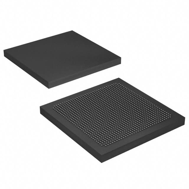
5SGXEA3K3F35I3N
Product Overview
- Category: Field Programmable Gate Array (FPGA)
- Use: Digital logic circuits, prototyping, and system integration
- Characteristics: High-performance, reconfigurable, programmable, and flexible
- Package: Integrated Circuit (IC)
- Essence: Advanced semiconductor device for implementing digital circuits
- Packaging/Quantity: Available in a single IC package
Specifications
- Manufacturer: Intel Corporation
- Family: Stratix V
- Device: 5SGXEA3K3F35I3N
- Technology: 28nm
- Logic Elements: 358,200
- Embedded Memory: 13,749 Kbits
- DSP Blocks: 2,530
- Transceivers: 48
- I/O Pins: 1,040
- Operating Voltage: 0.9V - 1.1V
- Operating Temperature: -40°C to 100°C
Detailed Pin Configuration
The 5SGXEA3K3F35I3N FPGA has a complex pin configuration with multiple I/O banks, power supply pins, and configuration pins. The detailed pin configuration can be found in the manufacturer's datasheet.
Functional Features
- High-speed performance: The FPGA offers high-speed processing capabilities, making it suitable for applications requiring real-time data processing.
- Reconfigurability: The device can be programmed and reprogrammed to implement different logic functions, allowing flexibility in system design.
- Integration: The FPGA integrates various components such as logic elements, memory blocks, and DSP units, reducing the need for external components.
- Low power consumption: The device is designed to operate efficiently, minimizing power consumption while maintaining high performance.
Advantages and Disadvantages
Advantages: - Flexibility: The reconfigurable nature of the FPGA allows for quick design iterations and modifications. - High performance: The FPGA's parallel processing capabilities enable high-speed data processing. - Integration: The integration of various components simplifies system design and reduces board space requirements.
Disadvantages: - Complexity: Working with FPGAs requires expertise in digital logic design and programming languages. - Cost: FPGAs can be more expensive compared to other programmable logic devices. - Power consumption: While efforts have been made to reduce power consumption, FPGAs still consume more power compared to dedicated ASICs.
Working Principles
The 5SGXEA3K3F35I3N FPGA operates based on the principles of configurable logic. It consists of an array of programmable logic elements interconnected through a network of configurable routing resources. These logic elements can be programmed to implement desired digital circuits by configuring their interconnections and functionality.
The device is programmed using Hardware Description Languages (HDL) such as VHDL or Verilog. The HDL code describes the desired circuit behavior, which is then synthesized into a configuration bitstream. This bitstream is loaded into the FPGA, configuring its internal resources to realize the desired circuit functionality.
Detailed Application Field Plans
The 5SGXEA3K3F35I3N FPGA finds applications in various fields, including:
- Communications: Used in wireless base stations, routers, and network switches for high-speed data processing and protocol handling.
- Signal Processing: Employed in digital signal processing systems for real-time audio/video processing, image recognition, and radar/sonar applications.
- Industrial Automation: Utilized in control systems, robotics, and machine vision applications for high-performance control and data processing.
- Medical: Applied in medical imaging equipment, patient monitoring systems, and DNA sequencing for high-speed data processing and analysis.
- Aerospace and Defense: Used in radar systems, avionics, and military communication equipment for high-performance signal processing and encryption.
Detailed and Complete Alternative Models
- Altera (Intel) Stratix V 5SGXEA7K3F35C2N
- Xilinx Virtex-7 XC7VX690T-2FFG1761C
- Lattice Semiconductor ECP5-85
- Microsemi SmartFusion2 M2S090TS-1FGG484I
- QuickLogic PolarPro 3 S3LP036
These alternative models offer similar functionality and performance to the 5SGXEA3K3F35I3N FPGA and can be considered as alternatives based on specific project requirements.
Note: The content provided above is a sample structure for an encyclopedia entry and may not reflect actual specifications or details of the mentioned product.
Seznam 10 běžných otázek a odpovědí souvisejících s aplikací 5SGXEA3K3F35I3N v technických řešeních
Sure! Here are 10 common questions and answers related to the application of 5SGXEA3K3F35I3N in technical solutions:
Q: What is the 5SGXEA3K3F35I3N FPGA used for? A: The 5SGXEA3K3F35I3N is a Field-Programmable Gate Array (FPGA) that can be used for various applications such as high-performance computing, networking, and signal processing.
Q: What are the key features of the 5SGXEA3K3F35I3N FPGA? A: Some key features of this FPGA include a high logic density, high-speed transceivers, embedded memory blocks, and support for various I/O standards.
Q: Can the 5SGXEA3K3F35I3N FPGA be reprogrammed? A: Yes, FPGAs are designed to be reprogrammable, allowing users to modify the functionality of the device even after it has been deployed.
Q: How can the 5SGXEA3K3F35I3N FPGA be programmed? A: The 5SGXEA3K3F35I3N FPGA can be programmed using hardware description languages (HDLs) such as VHDL or Verilog, or through graphical programming tools provided by the FPGA manufacturer.
Q: What are some typical applications of the 5SGXEA3K3F35I3N FPGA? A: This FPGA can be used in applications such as high-frequency trading, software-defined networking, video processing, radar systems, and data center acceleration.
Q: Does the 5SGXEA3K3F35I3N FPGA support high-speed communication interfaces? A: Yes, this FPGA has built-in high-speed transceivers that support various protocols such as PCIe, Ethernet, and Serial RapidIO.
Q: Can the 5SGXEA3K3F35I3N FPGA interface with external memory devices? A: Yes, this FPGA has embedded memory blocks and can also interface with external memory devices such as DDR3 or DDR4 SDRAM.
Q: What is the power consumption of the 5SGXEA3K3F35I3N FPGA? A: The power consumption of this FPGA depends on the specific design and configuration, but it typically ranges from a few watts to tens of watts.
Q: Are there any development kits available for the 5SGXEA3K3F35I3N FPGA? A: Yes, the FPGA manufacturer provides development kits that include the necessary hardware and software tools to facilitate the design and testing process.
Q: Can the 5SGXEA3K3F35I3N FPGA be used in safety-critical applications? A: While FPGAs can be used in safety-critical applications, it is important to ensure proper design, verification, and validation processes are followed to meet the required safety standards.

