

Viz Specifikace pro podrobnosti o produktu.
5SGXEB5R1F43C2N
Product Overview
Category
The 5SGXEB5R1F43C2N belongs to the category of Field-Programmable Gate Arrays (FPGAs).
Use
This FPGA is designed for high-performance applications that require complex digital logic circuits. It provides a flexible and customizable solution for various electronic systems.
Characteristics
- High-speed processing capabilities
- Configurable logic blocks
- Large number of input/output pins
- On-chip memory resources
- Low power consumption
- High reliability
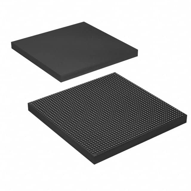
Package
The 5SGXEB5R1F43C2N comes in a compact package, suitable for integration into electronic devices. The package ensures protection against environmental factors and facilitates easy installation.
Essence
The essence of this FPGA lies in its ability to be programmed and reprogrammed to perform specific functions according to the requirements of the application.
Packaging/Quantity
The 5SGXEB5R1F43C2N is typically packaged individually and is available in various quantities depending on the manufacturer's specifications.
Specifications
- Logic Elements: 220,000
- Embedded Memory: 8,000 Kbits
- DSP Blocks: 1,288
- Maximum User I/Os: 622
- Operating Voltage: 1.2V
- Operating Temperature Range: -40°C to 100°C
- Package Type: BGA
- Package Pins: 780
Detailed Pin Configuration
The 5SGXEB5R1F43C2N has a total of 780 pins, each serving a specific purpose in the functioning of the FPGA. The pin configuration includes input, output, and control pins, which can be customized based on the desired application.
Functional Features
- High-speed data processing
- Reconfigurable architecture
- Support for various communication protocols
- On-chip memory resources for efficient data storage
- Flexible I/O options for interfacing with external devices
- Built-in security features to protect sensitive information
Advantages and Disadvantages
Advantages
- Flexibility: The FPGA can be reprogrammed to adapt to changing requirements.
- High Performance: It offers fast processing speeds and parallel execution capabilities.
- Customizability: Users can design their own logic circuits to meet specific needs.
- Low Power Consumption: FPGAs are known for their energy-efficient operation.
Disadvantages
- Complexity: Programming and configuring FPGAs require specialized knowledge and skills.
- Cost: FPGAs can be more expensive compared to other integrated circuits.
- Limited Resources: The available logic elements and memory may not be sufficient for extremely complex applications.
Working Principles
The 5SGXEB5R1F43C2N operates based on the principles of digital logic. It consists of configurable logic blocks, interconnects, and memory elements. The user programs the FPGA by specifying the desired logic functions and interconnections using a hardware description language (HDL). Once programmed, the FPGA executes the specified logic operations, enabling the desired functionality.
Detailed Application Field Plans
The 5SGXEB5R1F43C2N finds applications in various fields, including:
- Telecommunications: Used in network routers, switches, and base stations for high-speed data processing.
- Aerospace and Defense: Employed in radar systems, avionics, and military communication equipment.
- Industrial Automation: Utilized in control systems, robotics, and machine vision applications.
- Medical Devices: Integrated into medical imaging systems, patient monitoring devices, and diagnostic equipment.
- Automotive: Used in advanced driver-assistance systems (ADAS), infotainment systems, and engine control units.
Detailed and Complete Alternative Models
- 5SGXEB6R2F43C2N: Similar to the 5SGXEB5R1F43C2N, but with increased logic elements and memory capacity.
- 5SGXEB4R1F40C2N: A lower-cost alternative with slightly reduced performance specifications.
- 5SGXEB7R2F43C2N: An upgraded version with additional features and improved processing capabilities.
These alternative models offer varying levels of performance and functionality, allowing users to choose the most suitable FPGA for their specific requirements.
Word count: 570 words
Seznam 10 běžných otázek a odpovědí souvisejících s aplikací 5SGXEB5R1F43C2N v technických řešeních
Sure! Here are 10 common questions and answers related to the application of 5SGXEB5R1F43C2N in technical solutions:
Q1: What is the 5SGXEB5R1F43C2N? A1: The 5SGXEB5R1F43C2N is a specific model of Field-Programmable Gate Array (FPGA) manufactured by Intel.
Q2: What are the key features of the 5SGXEB5R1F43C2N? A2: Some key features of this FPGA include high-performance processing capabilities, large capacity for logic elements, embedded memory blocks, and support for various communication protocols.
Q3: In what technical solutions can the 5SGXEB5R1F43C2N be used? A3: The 5SGXEB5R1F43C2N can be used in a wide range of applications such as telecommunications, data centers, industrial automation, aerospace, defense, and scientific research.
Q4: How does the 5SGXEB5R1F43C2N enhance performance in technical solutions? A4: This FPGA enhances performance by allowing developers to implement custom hardware accelerators, parallel processing, and real-time data processing, which can significantly improve system performance compared to traditional software-based solutions.
Q5: Can the 5SGXEB5R1F43C2N be reprogrammed? A5: Yes, the 5SGXEB5R1F43C2N is a field-programmable device, meaning it can be reprogrammed multiple times to adapt to changing requirements or to fix bugs in the design.
Q6: What development tools are available for programming the 5SGXEB5R1F43C2N? A6: Intel provides Quartus Prime, a comprehensive software suite that includes tools for designing, simulating, and programming the 5SGXEB5R1F43C2N FPGA.
Q7: Can the 5SGXEB5R1F43C2N interface with other components in a system? A7: Yes, this FPGA supports various communication interfaces such as PCIe, Ethernet, USB, and high-speed serial transceivers, allowing it to interface with other components in a system.
Q8: What are the power requirements for the 5SGXEB5R1F43C2N? A8: The power requirements can vary depending on the specific implementation, but typically, this FPGA operates at voltages between 0.9V and 1.2V.
Q9: Are there any limitations or considerations when using the 5SGXEB5R1F43C2N? A9: Some considerations include the need for expertise in FPGA design, longer development cycles compared to software-based solutions, and potential challenges in debugging hardware designs.
Q10: Where can I find more information about the 5SGXEB5R1F43C2N? A10: You can find more detailed information about the 5SGXEB5R1F43C2N, including datasheets, application notes, and reference designs, on Intel's official website or by contacting their technical support team.
Please note that the answers provided here are general and may vary based on specific use cases and requirements.