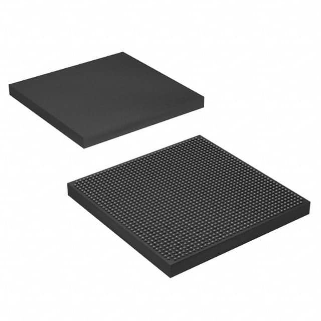
Viz Specifikace pro podrobnosti o produktu.

5SGXEB6R2F40C3
Product Overview
Category
The 5SGXEB6R2F40C3 belongs to the category of Field-Programmable Gate Arrays (FPGAs).
Use
FPGAs are integrated circuits that can be programmed or reprogrammed after manufacturing. They are widely used in various electronic applications, including telecommunications, automotive, aerospace, and industrial automation.
Characteristics
- High flexibility: FPGAs can be customized to perform specific tasks by programming their internal logic.
- Parallel processing: FPGAs can execute multiple operations simultaneously, making them suitable for high-performance computing.
- Reconfigurability: FPGAs can be reprogrammed to adapt to changing requirements or to fix errors without replacing the hardware.
- Low power consumption: FPGAs offer efficient power management features, enabling energy-efficient designs.
- Scalability: FPGAs come in different sizes and configurations, allowing designers to choose the most appropriate device for their application.
Package and Quantity
The 5SGXEB6R2F40C3 is available in a specific package type, which may vary depending on the manufacturer. The quantity per package also depends on the supplier's specifications.
Essence
The essence of the 5SGXEB6R2F40C3 lies in its ability to provide a highly flexible and customizable solution for complex digital designs. It allows designers to implement their own logic functions and algorithms, providing a versatile platform for various applications.
Packaging/Quantity
The 5SGXEB6R2F40C3 is typically packaged in a ceramic or plastic package, ensuring protection from external factors such as moisture and physical damage. The quantity per package may vary depending on the manufacturer's specifications.
Specifications
- FPGA Family: Stratix V
- Device Type: 5SGXEB6R2F40C3
- Logic Elements: 622,080
- Embedded Memory: 25,920 Kbits
- DSP Blocks: 1,288
- Maximum User I/Os: 1,040
- Operating Voltage: 1.0V
- Package Type: BGA (Ball Grid Array)
- Package Pins: 1517
Detailed Pin Configuration
The detailed pin configuration of the 5SGXEB6R2F40C3 can be found in the manufacturer's datasheet or technical documentation.
Functional Features
- High-performance FPGA with advanced architecture.
- Support for various communication protocols and interfaces.
- Built-in memory blocks for efficient data storage and retrieval.
- Dedicated digital signal processing (DSP) blocks for complex mathematical operations.
- Flexible clock management and synchronization capabilities.
- On-chip configuration memory for easy reprogramming.
Advantages and Disadvantages
Advantages
- High flexibility and customization options.
- Parallel processing capability for improved performance.
- Reconfigurability allows for easy updates and modifications.
- Low power consumption compared to traditional ASIC designs.
- Scalable to meet different application requirements.
Disadvantages
- Higher cost compared to fixed-function integrated circuits.
- Steeper learning curve for programming and design implementation.
- Limited resources and capacity compared to dedicated hardware solutions.
- Longer development time compared to off-the-shelf components.
Working Principles
The 5SGXEB6R2F40C3 operates based on the principles of reconfigurable logic. It consists of a matrix of configurable logic blocks interconnected through programmable routing resources. The device can be programmed using Hardware Description Languages (HDLs) such as VHDL or Verilog, which describe the desired functionality of the circuit. Once programmed, the FPGA executes the specified logic functions and algorithms.
Detailed Application Field Plans
The 5SGXEB6R2F40C3 finds applications in various fields, including:
- Telecommunications: FPGAs are used in base stations, routers, and network switches to handle high-speed data processing and protocol conversion.
- Automotive: FPGAs enable advanced driver assistance systems (ADAS), engine control units (ECUs), and infotainment systems.
- Aerospace: FPGAs are utilized in satellite communication systems, avionics, and flight control systems for their reliability and performance.
- Industrial Automation: FPGAs play a crucial role in industrial control systems, robotics, and machine vision applications.
- Medical Devices: FPGAs are employed in medical imaging equipment, patient monitoring systems, and laboratory instruments.
Detailed and Complete Alternative Models
- 5SGXEA7N2F45C2
- 5SGXEA7H2F35C2
- 5SGXEA9K2F40C2
- 5SGXEA9H2F35C2
- 5SGXEA9N2F45C2
These alternative models offer similar
Seznam 10 běžných otázek a odpovědí souvisejících s aplikací 5SGXEB6R2F40C3 v technických řešeních
Sure! Here are 10 common questions and answers related to the application of 5SGXEB6R2F40C3 in technical solutions:
Question: What is the 5SGXEB6R2F40C3 FPGA used for?
Answer: The 5SGXEB6R2F40C3 FPGA is a field-programmable gate array that can be used for various applications such as high-performance computing, networking, and signal processing.Question: What is the maximum number of logic elements in the 5SGXEB6R2F40C3 FPGA?
Answer: The 5SGXEB6R2F40C3 FPGA has a maximum of 622,080 logic elements.Question: Can the 5SGXEB6R2F40C3 FPGA support high-speed serial interfaces?
Answer: Yes, the 5SGXEB6R2F40C3 FPGA supports high-speed serial interfaces such as PCIe, SATA, and Ethernet.Question: What is the maximum operating frequency of the 5SGXEB6R2F40C3 FPGA?
Answer: The maximum operating frequency of the 5SGXEB6R2F40C3 FPGA is dependent on the specific design and implementation, but it can reach up to several hundred megahertz.Question: Can the 5SGXEB6R2F40C3 FPGA be reprogrammed?
Answer: Yes, the 5SGXEB6R2F40C3 FPGA is a field-programmable device, which means it can be reprogrammed multiple times to implement different designs or functionalities.Question: What development tools are available for programming the 5SGXEB6R2F40C3 FPGA?
Answer: The 5SGXEB6R2F40C3 FPGA can be programmed using Intel Quartus Prime software, which provides a comprehensive development environment for designing and programming FPGAs.Question: Can the 5SGXEB6R2F40C3 FPGA interface with external memory devices?
Answer: Yes, the 5SGXEB6R2F40C3 FPGA supports various memory interfaces such as DDR3, DDR4, and QDR IV, allowing it to interface with external memory devices.Question: What is the power consumption of the 5SGXEB6R2F40C3 FPGA?
Answer: The power consumption of the 5SGXEB6R2F40C3 FPGA depends on the specific design and operating conditions, but it typically ranges from a few watts to tens of watts.Question: Can the 5SGXEB6R2F40C3 FPGA be used in safety-critical applications?
Answer: Yes, the 5SGXEB6R2F40C3 FPGA can be used in safety-critical applications, provided that proper design techniques and safety measures are implemented.Question: Are there any reference designs or application notes available for the 5SGXEB6R2F40C3 FPGA?
Answer: Yes, Intel provides a wide range of reference designs, application notes, and documentation to help users get started with the 5SGXEB6R2F40C3 FPGA and implement their desired technical solutions.
Please note that the answers provided here are general and may vary depending on the specific requirements and use cases. It is always recommended to refer to the official documentation and datasheets for accurate and up-to-date information.

