

Viz Specifikace pro podrobnosti o produktu.
EP1C3T100C8
Product Overview
- Category: Programmable Logic Device (PLD)
- Use: EP1C3T100C8 is a PLD that can be programmed to perform various logic functions.
- Characteristics:
- High-speed performance
- Low power consumption
- Small form factor
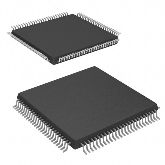
- Package: TQFP (Thin Quad Flat Package)
- Essence: The EP1C3T100C8 is designed to provide flexible and customizable logic functions in electronic systems.
- Packaging/Quantity: The EP1C3T100C8 is typically sold in reels or trays, with a quantity of 100 units per reel/tray.
Specifications
- Logic Elements: 3,000
- User I/O Pins: 78
- Embedded Memory: 4,608 bits
- Operating Voltage: 3.3V
- Operating Temperature: -40°C to 85°C
- Speed Grade: 8 (maximum frequency of 250 MHz)
Detailed Pin Configuration
The EP1C3T100C8 has a total of 100 pins, each serving a specific purpose. The pin configuration is as follows:
- Pin 1: VCCIO
- Pin 2: GND
- Pin 3: IO_0
- Pin 4: IO_1
- ...
- Pin 99: IO_96
- Pin 100: IO_97
Please refer to the datasheet for the complete pin configuration details.
Functional Features
- High-speed operation: The EP1C3T100C8 offers fast processing capabilities, making it suitable for applications requiring quick response times.
- Flexibility: The device can be programmed to implement a wide range of logic functions, allowing for customization based on specific requirements.
- Low power consumption: The EP1C3T100C8 is designed to minimize power usage, making it suitable for battery-powered devices or energy-efficient applications.
Advantages and Disadvantages
Advantages: - Versatility: The EP1C3T100C8 can be used in various applications due to its programmable nature. - Small form factor: The TQFP package allows for compact designs, saving valuable board space. - High-speed performance: The device offers fast processing capabilities, enabling efficient operation.
Disadvantages: - Limited logic elements: With 3,000 logic elements, the EP1C3T100C8 may not be suitable for complex designs requiring a larger number of logic functions. - Programming complexity: Configuring the device requires knowledge of hardware description languages and programming tools.
Working Principles
The EP1C3T100C8 utilizes programmable logic technology to implement logic functions. It consists of configurable logic blocks (CLBs), interconnect resources, embedded memory, and I/O pins. The CLBs can be programmed to perform various logic operations, such as AND, OR, XOR, etc., based on the user's requirements. The interconnect resources allow for the routing of signals between different CLBs and I/O pins. The embedded memory provides additional storage for data manipulation. By programming the device using hardware description languages, the desired logic functions can be implemented.
Detailed Application Field Plans
The EP1C3T100C8 finds applications in various fields, including:
- Embedded Systems: The device can be used in embedded systems to implement custom logic functions, such as control and communication interfaces.
- Industrial Automation: EP1C3T100C8 can be employed in industrial automation systems for tasks like process control, monitoring, and data acquisition.
- Communications: The PLD can be utilized in communication systems for signal processing, protocol implementation, and data encryption.
- Consumer Electronics: EP1C3T100C8 can be integrated into consumer electronic devices to enable custom functionality and enhance performance.
Detailed and Complete Alternative Models
- EP1C3T144C8
- EP1C3T144I7
- EP1C3T144I8
- EP1C3T144I6N
- EP1C3T144I7N
These alternative models offer similar features and capabilities as the EP1C3T100C8 but may have different package options or pin configurations.
Seznam 10 běžných otázek a odpovědí souvisejících s aplikací EP1C3T100C8 v technických řešeních
Sure! Here are 10 common questions and answers related to the application of EP1C3T100C8 in technical solutions:
Q1: What is EP1C3T100C8? A1: EP1C3T100C8 is a specific model of Field-Programmable Gate Array (FPGA) manufactured by Altera (now Intel). It is commonly used in various technical solutions.
Q2: What are the key features of EP1C3T100C8? A2: EP1C3T100C8 has 3,000 logic elements, 72Kbits of embedded memory, and supports various I/O standards. It also offers high-speed performance and low power consumption.
Q3: What are the typical applications of EP1C3T100C8? A3: EP1C3T100C8 is often used in applications such as digital signal processing, industrial automation, robotics, telecommunications, and embedded systems.
Q4: How can EP1C3T100C8 be programmed? A4: EP1C3T100C8 can be programmed using Hardware Description Languages (HDLs) like VHDL or Verilog. Design files are compiled into a bitstream that can be loaded onto the FPGA.
Q5: Can EP1C3T100C8 be reprogrammed? A5: Yes, EP1C3T100C8 is a reprogrammable FPGA. The design can be modified and reprogrammed multiple times, allowing for flexibility in system development.
Q6: What tools are required to program EP1C3T100C8? A6: To program EP1C3T100C8, you will need a development board or programmer compatible with Altera FPGAs, along with the appropriate software tools like Quartus Prime.
Q7: What is the power supply requirement for EP1C3T100C8? A7: EP1C3T100C8 typically operates at a voltage of 3.3V, but it also supports a wide range of voltages (e.g., 2.5V to 5V) for different I/O standards.
Q8: Can EP1C3T100C8 interface with other components or devices? A8: Yes, EP1C3T100C8 can interface with various components and devices through its I/O pins. It supports different protocols such as SPI, I2C, UART, and more.
Q9: Are there any limitations or considerations when using EP1C3T100C8? A9: Some considerations include the limited number of logic elements and memory available in EP1C3T100C8. Complex designs may require larger FPGAs.
Q10: Where can I find additional resources and support for EP1C3T100C8? A10: You can refer to the official Intel (formerly Altera) website for datasheets, application notes, reference designs, and community forums dedicated to FPGA development.
Please note that these answers are general and may vary depending on specific requirements and use cases.