

Viz Specifikace pro podrobnosti o produktu.
EP2AGX125DF25C4
Product Overview
Category
EP2AGX125DF25C4 belongs to the category of programmable logic devices (PLDs).
Use
This product is used for designing and implementing digital circuits in various applications.
Characteristics
- High-performance programmable logic device
- Offers flexibility and versatility in circuit design
- Provides efficient integration of complex digital systems
- Supports advanced features such as high-speed interfaces and embedded processors
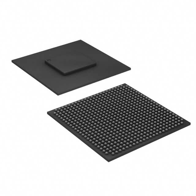
Package
EP2AGX125DF25C4 comes in a compact package that ensures easy installation and integration into electronic systems.
Essence
The essence of EP2AGX125DF25C4 lies in its ability to provide a customizable and reconfigurable solution for digital circuit design.
Packaging/Quantity
This product is typically packaged individually and is available in various quantities depending on the customer's requirements.
Specifications
- Device family: Arria II GX
- Device type: FPGA (Field-Programmable Gate Array)
- Logic elements: 125,000
- Embedded memory: 3,888 Kbits
- Maximum user I/O pins: 622
- Operating temperature range: -40°C to 100°C
- Supply voltage: 1.2V
Detailed Pin Configuration
The pin configuration of EP2AGX125DF25C4 is as follows:
- Pin 1: VCCIO
- Pin 2: GND
- Pin 3: CLKIN1_P
- Pin 4: CLKIN1_N
- Pin 5: CLKIN2_P
- Pin 6: CLKIN2_N
- ...
- Pin 622: IO622_B
For a complete list of pin configurations, please refer to the product datasheet.
Functional Features
EP2AGX125DF25C4 offers the following functional features:
- High-speed transceivers for data communication
- Embedded memory blocks for efficient storage and retrieval of data
- Programmable I/O pins for interfacing with external devices
- Dedicated digital signal processing (DSP) blocks for complex mathematical operations
- On-chip configuration memory for easy reprogramming
Advantages and Disadvantages
Advantages
- Flexibility in circuit design due to programmability
- High-performance capabilities for demanding applications
- Integration of multiple functions into a single device
- Cost-effective solution compared to custom-designed ASICs
Disadvantages
- Steeper learning curve for programming and utilizing the device's full potential
- Limited resources compared to larger FPGAs
- Higher power consumption compared to dedicated hardware solutions
Working Principles
EP2AGX125DF25C4 operates based on the principles of field-programmable gate arrays. It consists of configurable logic blocks (CLBs), interconnects, and various other components. The device can be programmed using hardware description languages (HDLs) such as VHDL or Verilog. Once programmed, the FPGA implements the desired digital circuit by configuring its internal resources.
Detailed Application Field Plans
EP2AGX125DF25C4 finds applications in various fields, including:
- Telecommunications: Used in base stations, network switches, and routers for high-speed data processing.
- Industrial Automation: Employed in control systems, robotics, and machine vision applications.
- Automotive: Utilized in advanced driver-assistance systems (ADAS) and infotainment systems.
- Aerospace and Defense: Integrated into radar systems, avionics, and secure communication equipment.
- Medical Devices: Used in medical imaging, patient monitoring, and laboratory equipment.
Detailed and Complete Alternative Models
Some alternative models to EP2AGX125DF25C4 include:
- EP2AGX190DF29C3: Offers higher logic capacity and additional features.
- EP4CE115F29C7: Provides a cost-effective solution with lower power consumption.
- XC7A35T-1CPG236C: A Xilinx FPGA with similar capabilities and performance.
These alternative models cater to different requirements and can be considered based on specific project needs.
Word count: 529 words
Seznam 10 běžných otázek a odpovědí souvisejících s aplikací EP2AGX125DF25C4 v technických řešeních
Sure! Here are 10 common questions and answers related to the application of EP2AGX125DF25C4 in technical solutions:
Q: What is EP2AGX125DF25C4? A: EP2AGX125DF25C4 is a specific model of field-programmable gate array (FPGA) manufactured by Intel.
Q: What are the key features of EP2AGX125DF25C4? A: EP2AGX125DF25C4 offers 125,000 logic elements, high-speed transceivers, embedded memory, and various I/O interfaces.
Q: What are some typical applications of EP2AGX125DF25C4? A: EP2AGX125DF25C4 is commonly used in telecommunications, industrial automation, aerospace, defense, and high-performance computing applications.
Q: How can EP2AGX125DF25C4 be programmed? A: EP2AGX125DF25C4 can be programmed using hardware description languages (HDLs) such as VHDL or Verilog, along with design software like Quartus Prime.
Q: Can EP2AGX125DF25C4 be used for real-time signal processing? A: Yes, EP2AGX125DF25C4's high-speed transceivers and embedded memory make it suitable for real-time signal processing applications.
Q: Does EP2AGX125DF25C4 support high-speed data transfer? A: Yes, EP2AGX125DF25C4 has built-in high-speed transceivers that support protocols like PCIe, Ethernet, and USB for fast data transfer.
Q: Can EP2AGX125DF25C4 interface with other components or devices? A: Yes, EP2AGX125DF25C4 supports various I/O standards and interfaces like GPIO, SPI, I2C, UART, and JTAG for seamless integration with other components.
Q: What are the power requirements for EP2AGX125DF25C4? A: EP2AGX125DF25C4 typically operates at a voltage range of 1.2V to 3.3V, depending on the specific design requirements.
Q: Is EP2AGX125DF25C4 suitable for low-power applications? A: While EP2AGX125DF25C4 is not specifically designed for low-power applications, power optimization techniques can be employed to reduce its power consumption.
Q: Are there any development boards or evaluation kits available for EP2AGX125DF25C4? A: Yes, Intel offers development boards and evaluation kits specifically designed for EP2AGX125DF25C4, which provide a convenient platform for prototyping and testing.
Please note that these answers are general and may vary based on specific implementation requirements and design considerations.