

Viz Specifikace pro podrobnosti o produktu.
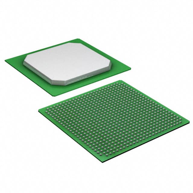
EP2C50F672C8
Product Overview
- Category: Programmable Logic Device (PLD)
- Use: EP2C50F672C8 is a PLD used for digital logic design and implementation.
- Characteristics:
- High-performance FPGA (Field-Programmable Gate Array) device
- Low power consumption
- Large capacity for complex designs
- Flexible and reprogrammable
- Package: The EP2C50F672C8 comes in a compact package suitable for surface mount technology.
- Essence: EP2C50F672C8 is an advanced programmable logic device that enables the implementation of complex digital circuits.
Specifications
- Logic Elements: 49,152
- Memory Bits: 1,966,080
- Embedded Multipliers: 288
- Maximum User I/O Pins: 622
- Operating Voltage: 1.2V
- Speed Grade: C8
Detailed Pin Configuration
The EP2C50F672C8 has a total of 622 user I/O pins, which can be configured as inputs or outputs based on the design requirements. These pins are distributed across different banks and support various voltage standards such as LVCMOS, LVTTL, and SSTL.
For a detailed pin configuration diagram, please refer to the official documentation provided by the manufacturer.
Functional Features
- High-speed performance: The EP2C50F672C8 offers fast signal processing capabilities, making it suitable for applications requiring real-time data processing.
- Reconfigurability: The device can be reprogrammed multiple times, allowing for flexibility in design modifications and updates.
- On-chip memory: The embedded memory blocks provide efficient storage for data-intensive applications.
- DSP Blocks: The integrated digital signal processing blocks enable efficient implementation of mathematical operations.
- Clock Management: The device includes clock management resources for precise timing control.
Advantages and Disadvantages
Advantages: - High capacity and flexibility for complex designs - Low power consumption - Reconfigurable nature allows for design modifications - On-chip memory and DSP blocks enhance performance
Disadvantages: - Steep learning curve for beginners due to the complexity of FPGA programming - Higher cost compared to traditional fixed-function integrated circuits - Limited availability of alternative models with similar specifications
Working Principles
The EP2C50F672C8 is based on FPGA technology, which utilizes a matrix of configurable logic blocks interconnected through programmable routing resources. The device can be programmed using Hardware Description Languages (HDLs) such as VHDL or Verilog. Once programmed, the FPGA configuration remains intact until reprogrammed.
The programmable nature of the EP2C50F672C8 allows designers to implement custom digital logic functions by configuring the interconnections between logic elements. This flexibility enables the device to adapt to various application requirements.
Detailed Application Field Plans
The EP2C50F672C8 finds applications in various fields, including:
- Telecommunications: Used in base stations, routers, and network switches for high-speed data processing.
- Industrial Automation: Enables control systems for robotics, motor drives, and process automation.
- Automotive: Utilized in advanced driver-assistance systems (ADAS), infotainment systems, and engine control units.
- Aerospace and Defense: Employed in radar systems, avionics, and secure communication systems.
- Medical Devices: Used in medical imaging equipment, patient monitoring systems, and laboratory instruments.
Alternative Models
While the EP2C50F672C8 offers unique specifications and features, there are alternative models available from other manufacturers that provide similar functionality. Some notable alternatives include:
- Xilinx XC7A100T-2FGG484C
- Intel (Altera) 10M08SAU169C8G
These alternative models offer comparable logic capacity, performance, and reconfigurability, providing designers with options based on their specific requirements.
Note: The above information is subject to change. For the most accurate and up-to-date details, please refer to the official documentation provided by the manufacturer.
Seznam 10 běžných otázek a odpovědí souvisejících s aplikací EP2C50F672C8 v technických řešeních
Sure! Here are 10 common questions and answers related to the application of EP2C50F672C8 in technical solutions:
Q: What is EP2C50F672C8? A: EP2C50F672C8 is a specific model of Field-Programmable Gate Array (FPGA) manufactured by Intel.
Q: What are the key features of EP2C50F672C8? A: Some key features of EP2C50F672C8 include 50,000 logic elements, 672 user I/O pins, and support for various communication protocols.
Q: How can EP2C50F672C8 be used in technical solutions? A: EP2C50F672C8 can be used in a wide range of applications such as digital signal processing, embedded systems, robotics, and high-performance computing.
Q: What programming languages can be used to program EP2C50F672C8? A: EP2C50F672C8 can be programmed using Hardware Description Languages (HDLs) like VHDL or Verilog.
Q: Can EP2C50F672C8 be reprogrammed after deployment? A: Yes, EP2C50F672C8 is a reprogrammable FPGA, allowing for flexibility and updates to the design even after deployment.
Q: What tools are available for designing with EP2C50F672C8? A: Intel provides Quartus Prime software suite, which includes tools for designing, simulating, and programming EP2C50F672C8.
Q: Are there any limitations to consider when using EP2C50F672C8? A: EP2C50F672C8 has limited resources, such as logic elements and I/O pins, so complex designs may require a larger FPGA.
Q: Can EP2C50F672C8 interface with other components or devices? A: Yes, EP2C50F672C8 supports various communication protocols like UART, SPI, I2C, and Ethernet, enabling interfacing with other components.
Q: What are the power requirements for EP2C50F672C8? A: EP2C50F672C8 typically operates at 1.2V core voltage and requires additional power supplies for I/O banks and configuration.
Q: Are there any development boards available for prototyping with EP2C50F672C8? A: Yes, Intel offers development boards like the DE2 series, which include EP2C50F672C8 and provide a platform for prototyping and testing.
Please note that these answers are general and may vary depending on specific use cases and requirements.