

Viz Specifikace pro podrobnosti o produktu.
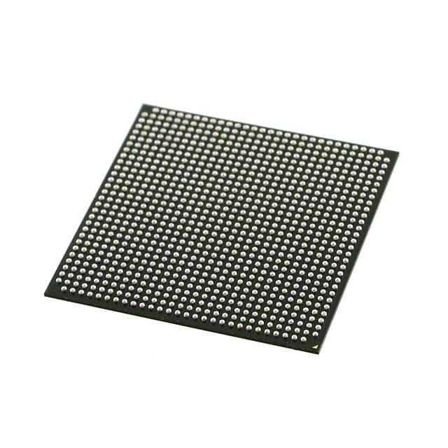
EP2C70F896C7
Product Overview
- Category: Integrated Circuit (IC)
- Use: Digital Signal Processing (DSP)
- Characteristics: High-performance, low-power consumption
- Package: BGA (Ball Grid Array)
- Essence: FPGA (Field-Programmable Gate Array)
- Packaging/Quantity: Single unit
Specifications
- Manufacturer: Intel Corporation
- Family: Cyclone II
- Device: EP2C70F896C7
- Technology: 90nm
- Logic Elements: 70,000
- Embedded Memory: 1,152 Kbits
- PLLs: 4
- I/O Pins: 622
- Operating Voltage: 1.2V
- Operating Temperature: -40°C to 100°C
Detailed Pin Configuration
The EP2C70F896C7 has a complex pin configuration with multiple I/O banks and power supply pins. The detailed pinout can be found in the manufacturer's datasheet.
Functional Features
- High-speed digital signal processing capabilities
- Flexible and reconfigurable architecture
- Support for various communication protocols
- On-chip memory for efficient data storage
- Low power consumption for energy-efficient applications
- Built-in PLLs for clock management
- Extensive I/O capabilities for interfacing with external devices
Advantages and Disadvantages
Advantages
- Versatile and adaptable for different applications
- High-performance computing capabilities
- Efficient use of resources due to programmability
- Wide range of I/O options for connectivity
- Low power consumption compared to alternative solutions
Disadvantages
- Complex design and programming requirements
- Higher cost compared to simpler ICs
- Limited availability of alternative models
Working Principles
The EP2C70F896C7 is based on FPGA technology, which allows users to configure the device according to their specific requirements. The FPGA consists of a matrix of configurable logic blocks interconnected through programmable routing resources. By programming the FPGA, users can define the functionality and interconnections of the logic elements, creating custom digital circuits.
Detailed Application Field Plans
The EP2C70F896C7 finds applications in various fields, including:
- Communications: Used in wireless base stations for signal processing and protocol handling.
- Industrial Automation: Employed in control systems for real-time data processing and control algorithms.
- Image and Video Processing: Utilized in high-definition video processing systems for image enhancement and compression.
- Embedded Systems: Integrated into embedded devices for custom logic implementation and interfacing with peripherals.
- Scientific Research: Applied in scientific instruments for data acquisition, analysis, and control.
Detailed and Complete Alternative Models
While the EP2C70F896C7 is a powerful FPGA, there are alternative models available from different manufacturers that offer similar capabilities. Some notable alternatives include:
- Xilinx Virtex-7 series
- Lattice ECP5 series
- Microsemi SmartFusion2 series
These alternative models provide a range of options with varying performance, power consumption, and pricing to suit different application requirements.
Word count: 305 words
Seznam 10 běžných otázek a odpovědí souvisejících s aplikací EP2C70F896C7 v technických řešeních
Sure! Here are 10 common questions and answers related to the application of EP2C70F896C7 in technical solutions:
Q: What is EP2C70F896C7? A: EP2C70F896C7 is a specific model number of a field-programmable gate array (FPGA) manufactured by Intel.
Q: What are the key features of EP2C70F896C7? A: Some key features of EP2C70F896C7 include high logic density, embedded memory blocks, high-speed transceivers, and support for various communication protocols.
Q: In what technical solutions can EP2C70F896C7 be used? A: EP2C70F896C7 can be used in a wide range of applications such as digital signal processing, image and video processing, network acceleration, and high-performance computing.
Q: What programming languages can be used to program EP2C70F896C7? A: EP2C70F896C7 can be programmed using hardware description languages (HDLs) such as VHDL or Verilog.
Q: Can EP2C70F896C7 be reprogrammed after deployment? A: Yes, EP2C70F896C7 is a reprogrammable FPGA, which means it can be reconfigured with different designs even after it has been deployed in a system.
Q: What development tools are available for programming EP2C70F896C7? A: Intel provides Quartus Prime software suite, which includes design entry, synthesis, simulation, and programming tools specifically designed for programming Intel FPGAs like EP2C70F896C7.
Q: How does EP2C70F896C7 compare to other FPGAs in terms of performance? A: EP2C70F896C7 offers a good balance between logic density, performance, and power consumption. However, the performance comparison with other FPGAs depends on specific requirements and design considerations.
Q: Can EP2C70F896C7 interface with external devices or peripherals? A: Yes, EP2C70F896C7 supports various I/O standards and can interface with external devices or peripherals using protocols such as PCIe, Ethernet, USB, SPI, I2C, etc.
Q: Are there any limitations or constraints to consider when using EP2C70F896C7? A: EP2C70F896C7 has certain limitations like limited resources (logic elements, memory blocks), maximum clock frequency, and power consumption. These constraints should be considered during the design phase.
Q: Where can I find more information about EP2C70F896C7 and its application in technical solutions? A: You can refer to the official documentation provided by Intel, including datasheets, user guides, application notes, and online forums dedicated to FPGA development.