Viz Specifikace pro podrobnosti o produktu.

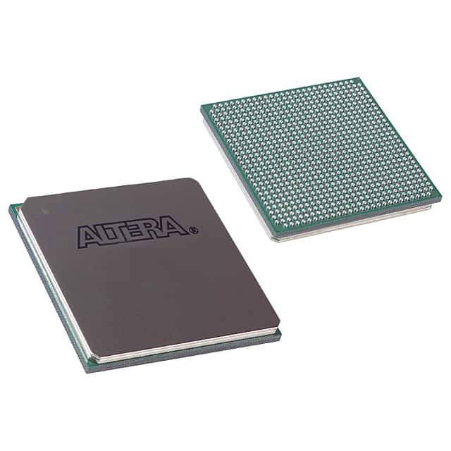
EP2SGX30DF780C4N
Product Overview
- Category: Integrated Circuit (IC)
- Use: Field Programmable Gate Array (FPGA)
- Characteristics: High-performance, low-power consumption
- Package: 780-pin Ceramic Flip Chip BGA
- Essence: Advanced programmable logic device
- Packaging/Quantity: Single unit per package
Specifications
- Manufacturer: Intel Corporation
- Series: Stratix II GX
- Model: EP2SGX30DF780C4N
- Technology: 90nm
- Number of Logic Elements: 29,440
- Number of Embedded Multipliers: 144
- Total Memory Bits: 1,152,000
- Operating Voltage: 1.2V
- Operating Temperature: -40°C to 100°C
- Speed Grade: 4
Detailed Pin Configuration
The EP2SGX30DF780C4N has a total of 780 pins arranged in a specific configuration. The pinout diagram and detailed pin descriptions can be found in the manufacturer's datasheet.
Functional Features
- High-speed performance with advanced logic elements
- Flexible and reconfigurable design for various applications
- Low power consumption for energy-efficient operation
- Built-in memory blocks for efficient data storage
- Support for high-speed serial transceivers
- On-chip PLLs for clock generation and synchronization
- Extensive I/O capabilities for interfacing with external devices
Advantages and Disadvantages
Advantages
- Versatile and adaptable for different applications
- High-performance computing capabilities
- Low power consumption for energy efficiency
- Ample memory resources for data storage
- Reliable and robust design
Disadvantages
- Relatively high cost compared to other FPGA options
- Limited availability of alternative models with similar specifications
Working Principles
The EP2SGX30DF780C4N is based on the field-programmable gate array (FPGA) technology. It consists of a large number of configurable logic blocks interconnected through programmable routing resources. The device can be programmed to implement various digital circuits and functions by configuring the interconnections and functionality of its logic elements.
Detailed Application Field Plans
The EP2SGX30DF780C4N finds applications in a wide range of fields, including:
- Telecommunications: Used in high-speed data transmission systems, network routers, and switches.
- Aerospace and Defense: Employed in radar systems, avionics, and military communication equipment.
- Industrial Automation: Utilized in control systems, robotics, and machine vision applications.
- Medical Devices: Integrated into medical imaging systems, patient monitoring devices, and diagnostic equipment.
- Automotive: Applied in advanced driver assistance systems (ADAS), infotainment systems, and engine control units.
Detailed and Complete Alternative Models
While the EP2SGX30DF780C4N offers unique features and specifications, there are alternative FPGA models available from different manufacturers that may suit specific requirements. Some notable alternatives include:
- Xilinx Virtex-7 XC7VX485T-2FFG1761C
- Lattice Semiconductor ECP5-85
- Microsemi SmartFusion2 M2S010-1FGG484I
These alternatives provide a range of options with varying capabilities and price points, allowing users to select the most suitable FPGA for their specific application needs.
Word count: 400 words
Seznam 10 běžných otázek a odpovědí souvisejících s aplikací EP2SGX30DF780C4N v technických řešeních
Sure! Here are 10 common questions and answers related to the application of EP2SGX30DF780C4N in technical solutions:
Question: What is EP2SGX30DF780C4N?
Answer: EP2SGX30DF780C4N is a specific model of field-programmable gate array (FPGA) manufactured by Intel.Question: What are the key features of EP2SGX30DF780C4N?
Answer: Some key features of EP2SGX30DF780C4N include high-performance logic fabric, embedded memory blocks, high-speed transceivers, and support for various I/O standards.Question: In what applications can EP2SGX30DF780C4N be used?
Answer: EP2SGX30DF780C4N can be used in a wide range of applications such as telecommunications, networking, industrial automation, aerospace, and defense.Question: How does EP2SGX30DF780C4N compare to other FPGAs?
Answer: EP2SGX30DF780C4N offers a good balance between performance, power consumption, and cost, making it suitable for many mid-range to high-end applications.Question: What development tools are available for EP2SGX30DF780C4N?
Answer: Intel provides Quartus Prime software suite, which includes design entry, synthesis, simulation, and programming tools specifically tailored for EP2SGX30DF780C4N.Question: Can EP2SGX30DF780C4N be reprogrammed after deployment?
Answer: Yes, EP2SGX30DF780C4N is a reprogrammable FPGA, allowing for flexibility and adaptability in the field.Question: What is the maximum operating frequency of EP2SGX30DF780C4N?
Answer: The maximum operating frequency of EP2SGX30DF780C4N depends on the specific design and implementation, but it can reach several hundred megahertz or even gigahertz.Question: Does EP2SGX30DF780C4N support high-speed serial communication protocols?
Answer: Yes, EP2SGX30DF780C4N has built-in high-speed transceivers that support protocols like PCIe, Ethernet, USB, and SATA.Question: Can EP2SGX30DF780C4N interface with external memory devices?
Answer: Yes, EP2SGX30DF780C4N has embedded memory blocks and supports various external memory interfaces such as DDR3, DDR4, and QDR IV.Question: Are there any reference designs or application notes available for EP2SGX30DF780C4N?
Answer: Yes, Intel provides a wide range of reference designs, application notes, and documentation to help users get started with EP2SGX30DF780C4N and implement their technical solutions efficiently.
Please note that the answers provided here are general and may vary depending on the specific requirements and use cases. It's always recommended to refer to the official documentation and consult with experts for detailed information.

