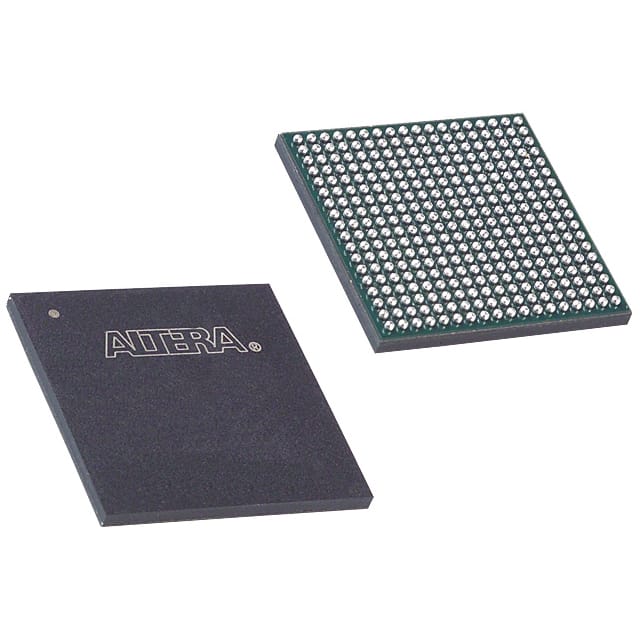
Viz Specifikace pro podrobnosti o produktu.

EP3C25F324C7
Product Overview
- Category: Programmable Logic Device (PLD)
- Use: EP3C25F324C7 is a PLD that can be programmed to perform various logic functions.
- Characteristics: It offers high performance, low power consumption, and flexibility in designing digital circuits.
- Package: The EP3C25F324C7 comes in a compact 324-ball FineLine BGA package.
- Essence: This PLD is designed to provide efficient and reliable programmable logic solutions for a wide range of applications.
- Packaging/Quantity: The EP3C25F324C7 is typically sold individually or in small quantities.
Specifications
- Logic Elements: The EP3C25F324C7 contains 24,624 logic elements.
- Embedded Memory: It includes 1,288 Kbits of embedded memory.
- PLLs: The device features four phase-locked loops (PLLs) for clock management.
- I/O Pins: It provides 324 I/O pins for interfacing with external devices.
- Operating Voltage: The recommended operating voltage is 1.2V.
- Speed Grade: The EP3C25F324C7 is available in different speed grades, such as -6, -7, and -8.
Pin Configuration
The EP3C25F324C7 has a detailed pin configuration, which can be found in the manufacturer's datasheet.
Functional Features
- High Performance: The EP3C25F324C7 offers fast operation and efficient utilization of resources.
- Low Power Consumption: It is designed to minimize power consumption, making it suitable for battery-powered applications.
- Flexibility: The PLD allows users to program and reprogram the device to meet specific requirements.
- Clock Management: The four PLLs enable precise clock generation and synchronization.
Advantages and Disadvantages
Advantages: - High performance and flexibility - Low power consumption - Compact package size - Extensive I/O capabilities
Disadvantages: - Limited embedded memory compared to some other PLDs - Higher cost compared to simpler logic devices
Working Principles
The EP3C25F324C7 operates based on the principles of programmable logic. It consists of configurable logic blocks (CLBs), interconnect resources, embedded memory, and I/O elements. Users can program the device using hardware description languages (HDL) or design software provided by the manufacturer. The programmed configuration is stored in non-volatile memory within the device and can be reprogrammed as needed.
Application Field Plans
The EP3C25F324C7 is suitable for a wide range of applications, including but not limited to: - Digital signal processing - Communication systems - Industrial automation - Consumer electronics - Automotive electronics
Alternative Models
There are several alternative models available that offer similar functionality to the EP3C25F324C7. Some popular alternatives include: - EP3C16F484C6 - EP4CE22F17C6N - EP2C20F484C7
These alternative models may have different specifications and pin configurations, so it is important to consult the respective datasheets for detailed information.
Word count: 346 words
Seznam 10 běžných otázek a odpovědí souvisejících s aplikací EP3C25F324C7 v technických řešeních
Sure! Here are 10 common questions and answers related to the application of EP3C25F324C7 in technical solutions:
Q: What is EP3C25F324C7? A: EP3C25F324C7 is a field-programmable gate array (FPGA) manufactured by Altera (now Intel). It offers 25,000 logic elements and is commonly used in various technical solutions.
Q: What are the key features of EP3C25F324C7? A: Some key features of EP3C25F324C7 include high-performance logic fabric, embedded memory blocks, digital signal processing (DSP) blocks, and support for various I/O standards.
Q: In what applications can EP3C25F324C7 be used? A: EP3C25F324C7 can be used in a wide range of applications such as industrial automation, telecommunications, automotive electronics, medical devices, and aerospace systems.
Q: How can EP3C25F324C7 be programmed? A: EP3C25F324C7 can be programmed using hardware description languages (HDLs) like VHDL or Verilog, which describe the desired functionality of the FPGA.
Q: Can EP3C25F324C7 be reprogrammed after deployment? A: Yes, EP3C25F324C7 is a reprogrammable FPGA, allowing for updates and modifications to the design even after it has been deployed in a system.
Q: What tools are available for designing with EP3C25F324C7? A: Intel Quartus Prime is the primary software tool used for designing, simulating, and programming EP3C25F324C7 FPGAs.
Q: What are the power requirements for EP3C25F324C7? A: EP3C25F324C7 typically operates at a voltage range of 1.2V to 3.3V, depending on the specific configuration and I/O standards used.
Q: Can EP3C25F324C7 interface with other components or devices? A: Yes, EP3C25F324C7 supports various communication protocols such as SPI, I2C, UART, and Ethernet, allowing it to interface with other components or devices in a system.
Q: Are there any limitations or considerations when using EP3C25F324C7? A: Some considerations include power consumption, heat dissipation, timing constraints, and the need for proper signal integrity and board layout design.
Q: Where can I find additional resources and support for EP3C25F324C7? A: Intel (formerly Altera) provides documentation, application notes, reference designs, and technical support through their website and community forums.

