

Viz Specifikace pro podrobnosti o produktu.
EP3C5E144I7
Product Overview
- Category: Integrated Circuit (IC)
- Use: Programmable Logic Device (PLD)
- Characteristics: Low-power, high-performance, small form factor
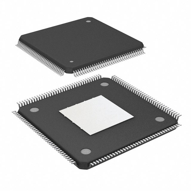
- Package: 144-pin Enhanced Plastic Quad Flat Pack (EPQFP)
- Essence: FPGA (Field-Programmable Gate Array)
- Packaging/Quantity: Available in reels of 250 units
Specifications
- Logic Elements: 5,136
- RAM Bits: 270,336
- Maximum User I/Os: 119
- Embedded Multiplier Blocks: 4
- Maximum Operating Frequency: 300 MHz
- Supply Voltage: 1.2V
- Operating Temperature Range: -40°C to 100°C
Detailed Pin Configuration
The EP3C5E144I7 has a total of 144 pins, each serving a specific purpose. The pin configuration includes power supply pins, ground pins, configuration pins, input/output pins, and dedicated pins for various functions such as clock input, reset, and programming.
For a detailed pin configuration diagram, please refer to the datasheet provided by the manufacturer.
Functional Features
- High-density programmable logic with abundant logic elements
- Flexible and reconfigurable design allowing for customization
- Low-power consumption for energy-efficient applications
- Fast operating speed for time-critical tasks
- Built-in memory blocks for efficient data storage
- Support for various communication protocols
- On-chip PLL (Phase-Locked Loop) for clock management
Advantages and Disadvantages
Advantages: - Versatile and adaptable for a wide range of applications - Compact size enables integration into space-constrained designs - Low-power consumption extends battery life in portable devices - High-performance capabilities meet demanding requirements - Cost-effective solution compared to custom ASIC designs
Disadvantages: - Limited number of I/O pins may restrict connectivity options - Programming and configuration process can be complex for beginners - FPGA designs require expertise in hardware description languages - Higher cost compared to traditional fixed-function integrated circuits
Working Principles
The EP3C5E144I7 is based on the FPGA technology, which allows users to configure the device according to their specific requirements. The device consists of an array of programmable logic elements interconnected through configurable routing resources. These logic elements can be programmed to implement various digital functions, such as arithmetic operations, data processing, and control logic.
The configuration of the EP3C5E144I7 is stored in non-volatile memory cells, which are loaded during power-up or reconfiguration. Once configured, the device operates based on the programmed logic, responding to input signals and generating output signals accordingly.
Detailed Application Field Plans
The EP3C5E144I7 finds applications in various fields, including but not limited to:
- Embedded Systems: Used for implementing custom logic in microcontroller-based systems.
- Communications: Enables protocol conversion, signal processing, and encryption/decryption tasks.
- Industrial Automation: Provides flexible control and monitoring capabilities for machinery and processes.
- Automotive Electronics: Supports advanced driver assistance systems (ADAS) and in-vehicle infotainment.
- Medical Devices: Facilitates real-time data acquisition, analysis, and control in medical equipment.
- Aerospace and Defense: Used in radar systems, avionics, and secure communication systems.
Detailed and Complete Alternative Models
- EP3C10E144I7: Similar to EP3C5E144I7 but with higher logic capacity and more I/O pins.
- EP3C16E144I7: Offers increased logic elements and memory capacity compared to EP3C5E144I7.
- EP3C25E144I7: Provides even higher logic density and additional features for complex designs.
- EP3C40E144I7: Suitable for applications requiring extensive logic resources and high-speed interfaces.
- EP3C80E144I7: Offers the highest logic capacity and performance in the EP3C series.
These alternative models provide a range of options with varying capabilities to suit different project requirements.
Word count: 550 words
Seznam 10 běžných otázek a odpovědí souvisejících s aplikací EP3C5E144I7 v technických řešeních
Sure! Here are 10 common questions and answers related to the application of EP3C5E144I7 in technical solutions:
Q: What is EP3C5E144I7? A: EP3C5E144I7 is a specific model of Field-Programmable Gate Array (FPGA) manufactured by Intel.
Q: What are the key features of EP3C5E144I7? A: EP3C5E144I7 offers 5,136 logic elements, 270 Kbits of embedded memory, and 144-pin package options.
Q: How can EP3C5E144I7 be used in technical solutions? A: EP3C5E144I7 can be used for various applications such as digital signal processing, industrial automation, and embedded systems.
Q: What programming languages are supported by EP3C5E144I7? A: EP3C5E144I7 supports popular hardware description languages like VHDL and Verilog.
Q: Can EP3C5E144I7 be reprogrammed after deployment? A: Yes, EP3C5E144I7 is a reprogrammable FPGA, allowing for flexibility and updates in the field.
Q: What tools are available for designing with EP3C5E144I7? A: Intel Quartus Prime is the primary software tool used for designing and programming EP3C5E144I7.
Q: Are there any development boards or kits available for EP3C5E144I7? A: Yes, Intel provides development boards and kits specifically designed for EP3C5E144I7, which include necessary components for prototyping.
Q: Can EP3C5E144I7 interface with other electronic components? A: Yes, EP3C5E144I7 supports various communication protocols like SPI, I2C, UART, and GPIO, allowing it to interface with other components.
Q: What are the power requirements for EP3C5E144I7? A: EP3C5E144I7 typically operates at a voltage range of 1.15V to 1.25V, with additional power supply pins for different functionalities.
Q: Are there any limitations or considerations when using EP3C5E144I7? A: Some considerations include power consumption, heat dissipation, and the need for external components like voltage regulators and clock sources.
Please note that these answers are general and may vary depending on specific use cases and requirements.